Intel Smart 3 Advanced Boot Block
Flash Memory Family of 4-, 8- and 16-Mbit
Devices 28F400B3, 28F800B3 and 28F160B3
| Additional High Integration Boot Block Devices | 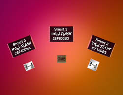 |
The Intel Smart 3 Advanced Boot Block family enables a new generation of low-power and lower cost applications by consolidating memory subsystems. This innovative flash memory family—the first of a new class of integrated code+data storage flash memory components—offers x16 devices for low-power code and EEPROM replacement in a single device. Each device is the most cost-effective solution for providing flexible data and code size, making it an ideal choice for applications such as digital cellular communication hand-sets, two-way messaging pagers, PCMCIA-card-based modems and networking cards, handheld organizers, and WLL subscriber units.
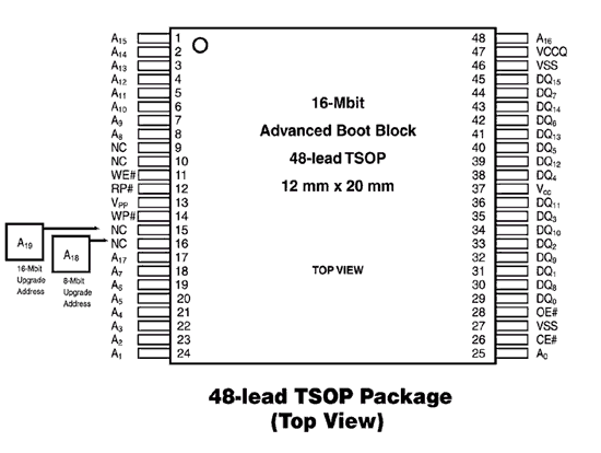
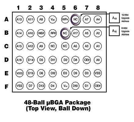
The Smart 3 Advanced Boot Block device is available in three densities of 4-, 8- and 16-Mbits. It is packaged in both the time-tested 48-lead TSOP and the newly developed 48-ball µBGA* package configurations. Using the same package pinout, designs can migrate easily from one density to another. Ready for use in current SMT production lines, Intel's µBGA package die functions as the package itself, offering the ultimate in package miniaturization. Intel's µBGA packaging uses a standard foot-print for upgradability and has been fully tested for maximum speed and minimum noise.
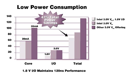
Smart 3 Advanced Boot Block Flash memory extends SmartVoltage technology with a read/write and erase voltage range of 2.7V to 3.6V for simplified low-voltage system design. Optional 12Vpp can increase device programming throughput, decreasing per-unit manufacturing costs. In addition, a new 1.8V I/O option is available. In emerging 1.8V systems, the power consumption can be reduced up to 35% when I/O pins are placed in the 1.8V I/O mode. (2.7V on Vcc is still required.)
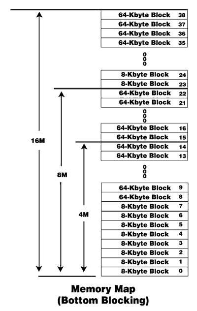
The Smart 3 Advanced Boot Block family also provides new blocking that simplifies the storage of code and data in a single device. Eight 8K byte blocks for data storage and up to 31 64K byte blocks are available for storing code or more data. Because write and erase timings are key to storing data and code in a single flash device, the Smart 3 Advanced Boot Block family has very fast write and erase suspend times, allowing the operating system to quickly return to executing code should a high-priority interrupt occur.
Intel Flash Data Integrator (FDI) software enables customers to easily and cost effectively use this memory component for both code and data storage. As FDI software allows code and data sizes to be user-defined, no hardware re-design is required as system needs change.
Designs using today's Boot Block flash memory family can be upgraded to the more cost-effective Smart 3 Advanced Boot Block family with only minor board design changes.
Product Highlights
|
| FEATURES | BENEFITS |
| SmartVoltage Technology multiple Voltage options 2.7V to 3.6V read/write/erase simplifies designs |
|
| Advanced Block architecture |
|
| Fast erase (13µs) and write (6µs) suspend |
|
| 4-, 8- and 16-Mbit compatible footprint |
|
| µBGA packaging |
|
| FDI Software |
|
 |
 |
 |
 |
| OTHER RELATED COLLATERAL | |
| ITEMS | DESCRIPTION |
| Datasheet | Smart 3 Advanced Boot Block Flash Memory Family |
| Application Note (AP-641) | Achieving Low Power with Advanced Boot Block Flash Memory |
| Application Note (AP-642) | Designing for Upgrade to Smart 3 Advanced Boot Block Flash Memory |
| User's Guide | Flash Data Integrator (FDI) User's Guide |
| Product Brief | Intel Flash Data Integrator (FDI) Developer's Kit |
Legal Stuff© 1997 Intel Corporation
