Intel Boot Block Flash Memory for PC BIOS 28F001BX, 28F002BC and 28F004BV
|
Additional High Integration Boot Block Devices Smart 3 Advanced Boot Block Flash Memory Family Smart 5 Boot Block Flash Memory Family Intel Blocked Flash Memory 28F001BX-B/28F001BX-T Intel's SmartVoltage Boot Block 2-, 4-, 8-Mbit Family | 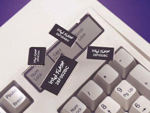
|
Product Description
Intel's 1-, 2- and 4-Megabit Boot Block Flash Memory devices are ideally suited for PC BIOS. The update capability of flash combined with the lockable boot block ensures safe BIOS updates from the manufacturing floor to the end-user. In addition, integrated parameter blocks provide an excellent solution for updating small code/data modules.
The 28F001BX Boot Block flash device is organized as 128Kbytes x8bits and is sectored into four blocks: one 8K hardware lockable boot block, two 4K parameter blocks and one 112K main block. The function of the 8K lockable boot block is to store system recovery code. This is the basic code necessary to boot the system. When the boot block is programmed during manufacturing, the write-protection pin is then used to lock out the boot block from reprogramming, effectively functioning as a ROM. The large main block contains runtime BIOS, video BIOS, multiple language support and other elements.
The two parameter blocks are used to store code/data that is frequently updated. Such information includes Extended System Configuration Data (ESCD) for Plug-and-Play, Desktop Management Interface (DMI) parameters, logos, user information and more. The parameter blocks provide an easy, safe way to update small code/data segments.
The 28F002BC device is organized as 256Kbytes x8bits and is sectored into five blocks: one 16K hardware lockable boot block, two 8K parameter blocks and two main blocks (96K/128K). The 28F002BC is manufactured on the 0.6µ process and optimized for the PC BIOS market segment, making it the lowest cost 2-Mbit component that Intel offers. This device is available in 80/120ns, top boot, TSOP/PSOP/PDIP packages and commercial temperature. The 28F002BC also supports 12V write, which allows fast programming during manufacturing or in-system updates.
The 28F002BC's blocking and functionality are similar to that of the 28F001BX. However, the doubling of density allows PC OEMs to incorporate more features into the PC platform. Such features include Universal Serial Bus, DMI, advanced diagnostics, integrated video and more.
The 28F004BV Boot Block device is organized as 512Kbytes x8bits and is sectored into seven blocks: one 16K hardware lockable boot block, two 8K parameter blocks and four main blocks (one 96K, three 128K). The 28F004BV is based on Intel's SmartVoltage technology, allowing read operations at 3.3V or 5V, and write operation at 5V or 12V. This provides maximum product design and manufacturing flexibility. The 28F004BV is used primarily in notebook computers which require additional BIOS for power management, PCMCIA and other elements.
- Integrated block architecture
- Byte-wide operation
- 3.3V and 5V read options
- 5V and 12V write options
- Surface mount and socketable packaging options
| FEATURES | BENEFITS |
| Lockable boot block |
|
| High-integration blocked architecture |
|
| Automated byte-write/block-erase |
|
| Erase suspend capability |
|
| 0.2 µA low-power sleep mode |
|
| 28F001BX | 28F002BC(1) | 28F004BV(2) | |
|---|---|---|---|
| Organization | x8 | x8 | x8 |
| Vcc/Vpp | 5/12V | 5/12V | 5/12, 3/12, 5/5, 3/5V |
| Packaging Options | 32-lead PDIP | 40-lead TSOP | 40-lead TSOP |
| 32-lead PLCC | 44-lead PSOP | ||
| 32-lead TSOP | 40-lead PDIP | ||
| (1) 28F002BV 2-Mbit SmartVoltage available for low power designs (5/12, 3/12, 5/5, 3/5V). (2) 28F400BV 4-Mbit SmartVoltage available for x8/x16 selectable, 44-ld PSOP, 48-ld TSOP and 56-ld TSOP. | |||
| Byte Address | PREVIOUS NEW | |
|---|---|---|
| 3FFFFH 3C000H | 16-Kbyte BOOT BLOCK | 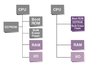
|
| 3BFFFH 3A000H | 8-Kbyte PARAMETER BLOCK | |
| 39FFFH 38000H | 8-Kbyte PARAMETER BLOCK | |
| 37FFFH 20000H | 96-Kbyte MAIN BLOCK | |
| 1FFFFH 00000H | 128-Kbyte MAIN BLOCK | |
EEPROM, Boot ROM and Bulk Erase Flash |
| ITEM | DESCRIPTION |
| Datasheet | 28F001BX-T, 28F001BX-B 1-Mbit Boot Block Flash Memory |
| Datasheet | 28F002BC 2-Mbit Boot Block Flash Memory |
| Datasheet | 28F004BV 4-Mbit SmartVoltage Boot Block Flash Memory |
| Datasheet | 28F002BV 2-Mbit SmartVoltage Boot Block Flash Memory |
| Application Note (AP-623) | Multi-Site Layout Planning With Intel's Boot Block Flash Memory |
297184-005
Intel Corporation assumes no responsibility for the use of any circuitry other than circuitry embodied in an Intel product. No other circuit patent licenses are implied. Information contained herein supersedes previously published specifications on these devices from Intel.
Legal Stuff © 1997 Intel Corporation
