SmartDie™ Products
|
|
SmartDie™ Manufacturing and Use
Overview
There are two commonly used methods for attaching IC dies to printed wiring boards: chip on board (COB) and flip-chip (also known as C-4: Controlled Collapse Chip Connection).
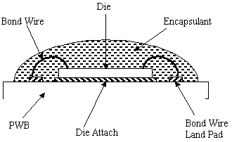
Chip on Board
One major benefit of COB is the ability to use standard FR4 PWBs.
Boards require gold-plating on the bond wire land pads to accommodate
wire bonding. This is accomplished by first placing a layer of
nickel on top of the copper, which provides a barrier layer to
prevent copper migration into the gold. The nickel also acts as
an anvil to stop penetration of the bond into the copper pad.
Gold plating typically adds 5 to 15 percent to the cost of the
PWB, depending on whether selective or non-selective plating is
required and depending on the board technology.
COB also gives designers the opportunity to trade off PWB trace
pitch for functional density. The area consumed by a COB device
varies proportionally with the pitch of the bond wire land pads.
In this equation, PWB fabrication costs can be weighed against
the advantages of increased functionality. On the downside, COB
allows for less space savings than flip-chip technology, because
bonding equipment requires approximately 30 mils between the land
pads and die edge, increasing the area consumed by COB devices.
Still, the space savings over standard packaging remains substantial.
Another advantage of COB over flip-chip is superior heat dissipation.
COB provides a large area of contact between the die and the PWB,
which provides a good path for thermal conduction and heat dissipation.
In contrast, the only connections between the board and die available
with flip-chip are the bumps on the bond pads, which provide a
poor path for heat transfer. Although you can place heat sinks
on the die substrate, this requires additional Z-height which
may not be desirable. These issues are discussed in more detail
in the chapter, "Thermal Considerations."
As integrated circuits mature, they often go through a "shrink"
process to reduce manufacturing costs. While this is transparent
to users of packaged devices, it requires planning for those using
die. COB minimizes the effects of stepping changes. In most situations,
it is possible for the manufacturer to simply increase the bond
wire length and continue using the same PWB.
Download one of the following .exe files to allow the windows "Media Player" to play the video files. After expanding the file in an empty directory, run the setup.exe which will automatically configure Media Player for .avi files.
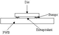
Flip-Chip Flip-chip die bonding involves placing bumps on die bond pads, typically with a tin-lead solder mixture. The tin-lead proportions vary and effect the mechanical and electrical properties of the bumps, as well as the solder reflow temperature. In assembly, the die is placed on the PWB with the IC circuitry facing the board (see Figure 2). The bumps are then reflowed, providing both the mechanical and electrical connection. The encapsulant provides a seal that protects the die from the environment, much like a separate package does.
Most of the advantages of flip-chip result from removing the wire between the die and the substrate. This allows higher package density than COB, because the connection to the substrate is directly with the die face. Using bumps instead of wires also increases reliability. Finally, performance increases because there's a shorter distance between bond pads and the substrate. Flip-chip is used by very few companies. Disadvantages include an unusual and expensive assembly process, which raises costs, and the possibility for thermal complications. One of the most common substrates in use, and the one used in COB, is FR-4. FR-4 corresponds to an MCM-Laminate (MCM-L) in multichip module terminology. When using FR-4, it is common to place die on both sides of the substrate to achieve higher density. FR-4 is the least expensive of the substrate options, because it uses commonly available printed wiring board materials. However, other substrate types should be considered because of the typically high coefficient of thermal expansion associated with FR-4/MCM-L. For example, if a design required gold wire bonds, then a substrate with a higher glass transition temperature (Tg) would be required in order to withstand the heat of the thermosonic gold wire bonding process. High Tg FR-4 material is available but at a cost. MCM-C, or ceramic-dielectric MCM technology, is the oldest of the MCM technologies. Thick-film ceramics and high and low-temperature co-fired ceramics use this technology. Al2O3, alumina, is the most popular ceramic material in use. MCM-Deposited (MCM-D) is a third option. MCM-D uses a deposition process to build the substrate. Its advantage is a very small trace pitch, which reduces the die footprint. The cost of MCM-D is much higher per square inch than MCM- L; however, the area consumed by MCM-D will be much less, offsetting the cost disadvantage to some degree. In a graph of circuit density vs. cost, the MCM-L curve will intersect the MCM-D curve at some point. The intersection point will depend on the application as well as the substrate manufacturer. Whether you should use MCM-D or MCM-L depends on whether space or cost savings is more important in your design.
Die and Surface Mount Technology (SMT) on Same Substrate
Tooling Requirements Many third-party contractors provide COB assembly services, eliminating the need for PC card OEMs to invest in this technology. Many also offer board design and layout services. These vendors can also manufacture a Ball-Grid Array (BGA) package using COB technology, and then attach it to a PC card using standard SMT techniques. Wire bonding is a mature process as it has been used for many years to assemble ICs in standard packages. As such, wire bonding equipment is readily available and costs from $20K for a manual bonder to approximately $250K for a high-speed automated bonder. Pick-and-place equipment is also needed for die attach and costs from $80K to $350K. Dispense equipment needed for encapsulation starts at about $30K and goes up to $100K. One drawback of COB is that it is a single unit processing step, i.e. only one wire bond connection can be made at a time. This requires an inherently slower process than SMT, which makes all electrical connections simultaneously. For high volume manufacturing, fully automated COB lines feed boards and components (including packaged components) into a machine and produce fully assembled boards.
Schematic Entry and Layout Tools
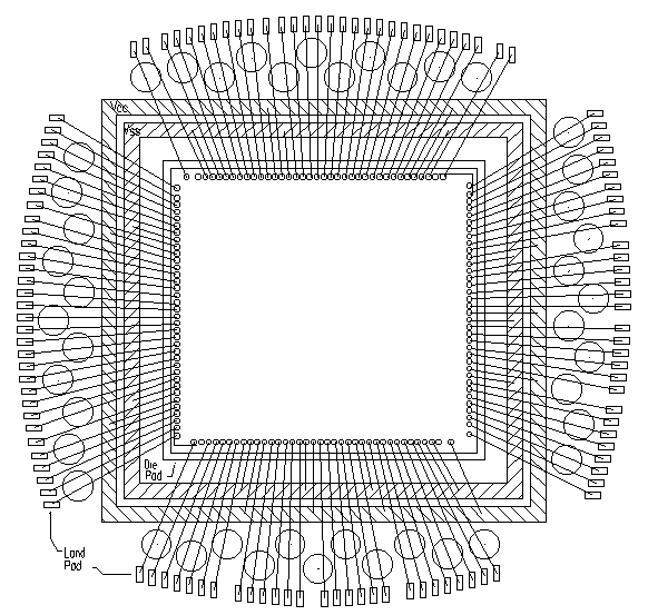
The issues of thermal performance must be considered during the layout phase of the design. One benefit of using die in a COB configuration is that the die substrate is directly accessible for heat dissipation. This is discussed further in the chapter, "Thermal Considerations." Manufacturability of COB is also a major concern. One challenge is how to handle the mismatch between the pitch of the bond pads, which can be as small as 3-4 mils, and the minimum pitch of the board traces, which are typically in the range of 8-10 mils. This mismatch requires creative layout of the bond wire land pads on the PWB. There are several options. Some designers stagger the land pads to meet the bond pad pitch. This minimizes the need to angle the bond wires but increases the bond wire length. This is caused by multiple rows of land pads and the need for vias to route the signals going to the internal lands. Another options is to use a radial land pad design, as shown in Figure 3. A radial design keeps all bond wires approximately the same length but causes the angle of the bondwires to increase as the bond pad is moved closer to the die corners. The effect of the bond wire angle on the land pad can be minimized if the land pad is rotated the same angle. The use of Vss and Vcc rings around the die reduces the number of land pads required for the design. This is especially beneficial for designs requiring a large number of power and ground bond pads. The use of rings also requires fewer vias to the power planes, but the bond wire length must be increased to allow room for the rings.
|

 |
|
Figure 3: Radial Land Pad Layout with
Vcc and Vss Rings
It is imperative that assembly technicians be involved in this aspect of the design. Specific parameters, some of which are listed below, are dependent upon the assembly equipment available and capabilities of the operators. Without understanding these limitations, manufacturability can be severely jeopardized.
Bond Wire Length
Bond Wire Angle
Land Pad Dimensions
Spacing Between Bonds and Adjacent Components
Bond Pad Pitch
Spacing Between Die Pad and Adjacent Metal To perform wire bonding, all wire bonding surfaces must be gold-plated. This adds two plating operations to the standard FR-4 fabrication process: nickel, which acts as a barrier layer between copper and gold, and the gold layer itself. If you do not want gold on all exposed surfaces, then you will also need a selective etch step.
Modeling The speed and volume advantages of MCM technology come at the expense of higher heat flux and increased failures. One of the most important considerations is keeping the IC junction temperature within its optimum temperature ranges. If the junction temperature exceeds its rated specifications no other performance specifications can be guaranteed. The junction temperature is equal to the ambient temperature plus the product of the component power dissipation and the junction-ambient thermal resistance. Several factors affect the junction temperatures, including the thermal resistance of encapsulation, the effects of surrounding components, and the type of heat removal used.
Heat Removal Strategies Heat removal techniques currently in use include heat pipes, aluminum plates, fan-sinks, and heat sinks combined with improved ventilation. A heat pipe is a two-phase liquid cooling device which works through evaporation and condensation. One side of the heat pipe contacts the heat source and the other side contacts a cold source (outside air). The water in the heat pipe boils where the heat source is applied, then evaporates. The vapor travels to cooler areas in the heat pipe, where the vapor condenses. The fluid then circulates back to the heat source through capillary action provided by wick structures along the inner walls of the heat pipe, and the cycle repeats. The performance of a heat pipe increases as its length decreases and diameter increases. Heat pipes are also more effective if they are straight rather than curved. Aluminum plates effectively spread heat over a larger area, thus enhancing convective heat transfer. Heat sinks are effective because in addition to providing a larger surface area for natural convection, they also increase the chimney effect to further enhance natural convection. Improvements brought about by heat sinks are limited if there is no low thermal resistance path to the ambient air, i.e. ventilation. You can mount a fan on top of the heat sink to provide forced convection, allowing the system to cool faster than if you depend on natural convection. A fan-sink is a single integrated component rather than two separate components (as a heat sink is). Power consumption, size, noise, and reliability are the drawbacks of fans.
Test Considerations Boundary scan implementations are compatible with the IEEE Standard Test Access Port and Boundary Scan Architecture (IEEE std. 1149.1). Boundary scan provides test access to a device via 4/5 common pins and gives a serial test path to all devices with scan on the module. Boundary scan allows for testing to insure that components function properly and that all interconnections are connected correctly. For more information on boundary scan see I.E.E.E. Standard Test Access Port and Boundary-Scan Architecture, Std 1149.1-1990, (Feb. 15, 1990), Copyright I.E.E.E. Inc. Built-in Self Test (BIST) consists of adding circuitry that allows a chip to test itself. The added circuitry, when activated, takes control, drives the inputs, observes the outputs, and reports whether the result is correct. BIST is often used on portions of the circuit that cannot be easily tested using another method. Also, even for parts of the circuit that can be tested for high fault coverage, BIST should be used if it reduces Burn-In or test cost. In line testing must be incorporated into the assembly flow in order to check for assembly defects or non-functional die prior to encapsulation. This will allow rework of the MCM and avoid scrapping non-defective ICs.
Programming Non-Volatile Memory
Design for Rework
Debug Considerations Sources for more information beyond the scope of this guide can be found in "Guidelines for Multichip Module Technology Utilization" IPC-MC-790 which was developed by the Institute for Interconnecting and Packaging Electronic Circuits. More information can also be found in "Guidelines for Chip-on-Board Technology Implementation", ANSI/IPC-SM-784, which is a standard also developed by the IPC.
|
Legal Stuff © 1997 Intel Corporation
