
Chapter 3
GUIDELINES FOR DEVELOPING MMX™ CODE
The following guidelines will help you develop fast and efficient MMX code that scales well across all processors with MMX technology.
The following section provides a list of rules and suggestions.
This section covers general optimization techniques that are important for the Intel Architecture.
On the Pentium processor, when a register is used as the base component, an additional clock cycle is used if that register is the destination of the immediately preceding instruction (assuming all instructions are already in the prefetch queue). For example:
add  esi, eax    ; esi is destination register
mov  eax, [esi]  ; esi is base, 1 clock penalty
Since the Pentium processor has two integer pipelines, a register used as the base or index component of an effective address calculation (in either pipe) causes an additional clock cycle if that register is the destination of either instruction from the immediately preceding clock cycle. This effect is known as Address Generation Interlock or AGI. To avoid the AGI, the instructions should be separated by at least one cycle by placing other instructions between them. The new MMX registers cannot be used as base or index registers, so the AGI does not apply for MMX register destinations.
Dynamic execution (P6-family) processors incur no penalty for the AGI condition.
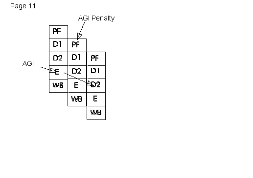
Note that some instructions have implicit reads/writes to registers. Instructions that generate addresses implicitly through ESP (PUSH, POP, RET, CALL) also suffer from the AGI penalty. Examples follow:
sub  esp, 24
        	;  1 clock cycle stall
push ebx
mov  esp, ebp
        	;1  clock cycle stall
pop  ebp
PUSH and POP also implicitly write to esp. This, however, does not cause an AGI when the next instruction addresses through ESP. Pentium processors "rename" ESP from PUSH and POP instructions to avoid the AGI penalty. An example follows:
push edi   	; no stall
mov  ebx, [esp]
On Pentium processors with MMX technology, instructions which include both an immediate and displacement fields are pairable in the U-pipe. When it is necessary to use constants, it is usually more efficient to use immediate data instead of loading the constant into a register first. If the same immediate data is used more than once, however, it is faster to load the constant in a register and then use the register multiple times. Following is an example:
mov  result, 555			; 555 is immediate, result is
					; displacement
mov  word ptr [esp+4], 1 		; 1 is immediate,4 is displacement
Since MMX instructions have two-byte opcodes (0x0F opcode map), any MMX instruction which uses base or index addressing with a 4-byte displacement to access memory will have a length of eight bytes. Instructions over seven bytes can limit decoding and should be avoided where possible (see Section 3.4.2). It is often possible to reduce the size of such instructions by adding the immediate value to the value in the base or index register, thus removing the immediate field.
The Intel486TM processor has a one clock penalty when using a full register immediately after a partial register was written. The Pentium processor is neutral in this respect. This is called a partial stall condition. The following example relates to the Pentium processor.
mov  al, 0           ; 1
mov  [ebp], eax      ; 2 - No delay on the Pentium processor
The following example relates to the Intel486 processor.
mov  al, 0 		; 1
 			; 2  1 clock penalty
mov  [ebp], eax		; 3
Dynamic execution (P6-family) processors exhibit the same type of stall as the Intel486 processors, except that the cost is much higher. The read is stalled until the partial write retires, which can be considerably longer than one clock cycle.
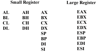
For best performance, avoid using a large register (for example, EAX) after writing a partial register (for example, AL, AH, AX) which is contained in the large register. This guideline will prevent partial stall conditions on dynamic execution processors and applies to all of the small and large register pairs:
AL	AH	AX	EAX
BL	BH	BX	EBX
CL	CH	CX	ECX
DL	DH	DX	EDX
		SP	ESP
		EP	EBP
		SI	ESI
		DI	EDI
Additional information on partial register stalls is in Section 3.2.4.
This section provides information on aligning code and data for Pentium and dynamic execution (P6-family) processors.
3.2.2.1 Code
Pentium and dynamic execution (P6-family) processors have a cache line size of 32 bytes. Since the prefetch buffers fetch on 16-byte boundaries, code alignment has a direct impact on prefetch buffer efficiency.
For optimal performance across the Intel Architecture family, it is recommended that:
3.2.2.2 Data
A misaligned access in the data cache or on the bus costs at least three extra clock cycles on the Pentium processor. A misaligned access in the data cache, which crosses a cache line boundary, costs nine to twelve clock cycles on dynamic execution (P6-family) processors. Intel recommends that data be aligned on the following boundaries for the best execution performance on all processors:
3.2.2.2.1 2-Byte Data
A 2-byte object should be fully contained within an aligned 4-byte word (that is, its binary address should be xxxx00, xxxx01, xxxx10, but not xxxx11).
3.2.2.2.2 4-Byte Data
The alignment of a 4-byte object should be on a 4-byte boundary.
3.2.2.2.3 8-Byte Data
An 8-byte datum (64 bit, for example, double precision real data types, all MMX packed register values) should be aligned on an 8-byte boundary.
On Pentium processors, a prefix on an instruction can delay the parsing and inhibit pairing of instructions.
The following list highlights the effects of instruction prefixes on the FIFO:
The impact on performance exists only when the FIFO does not hold at least two entries. As long as the decoder (D1 stage) has two instructions to decode there is no penalty. The FIFO will quickly become empty if the instructions are pulled from the FIFO at the rate of two per clock cycle. So, if the instructions just before the prefixed instruction suffer from a performance loss (for example, no pairing, stalls due to cache misses, misalignments, etc.), then the performance penalty of the prefixed instruction may be masked.
On dynamic execution (P6-family) processors, instructions longer than seven bytes in length limit the number of instructions decoded in each cycle (see Section 2.1.2). Prefixes add one to two bytes to the length of an instruction, possibly limiting the decoder.
It is recommended that, whenever possible, prefixed instructions not be used or that they be scheduled behind instructions which themselves stall the pipe for some other reason.
See Section 3.3 for more information on pairing of prefixed instructions.
On dynamic execution (P6-family) processors, when a 32-bit register (for example, EAX) is read immediately after 16 or 18-bit register (for example, AL, AH, AX) is written, the read is stalled until the write retires (a minimum of seven clock cycles). Consider the example below. The first instruction moves the value 8 into the AX register. The following instruction accesses the large register EAX. This code sequence results in a partial register stall.
MOV AX, 8
ADD ECX, EAX
Partial Stall occurs on access of the EAX register
This applies to all of the 8- and 16-bit/32-bit register pairs:
Pentium processors do not exhibit this penalty.
Because P6-family processors can execute code out of order, the instructions need not be immediately adjacent for the stall to occur. The following example also contains a partial stall:
MOV AL, 8
MOV EDX, 0x40
MOV EDI, new_value
ADD EDX, EAX
Partial Stall Occurs on access of the EAX register
In addition, any micro-ops that follow the stalled micro-op will also wait until the clock cycle after the stalled micro-op continues through the pipe. In general, to avoid stalls, do not read a large (32-bit) register (EAX) after writing a small (16- or 18-bit) register (AL) which is contained in the large register.
Special cases of reading and writing small and large register pairs have been implemented in dynamic execution processors in order to simplify the blending of code across processor generations. The special cases include the XOR and SUB instructions as shown in the following examples:
    xor  eax, eax
    movb  al, mem8
    use  eax  <------- no partial stall

    xor  eax, eax
    movw  ax, mem16
    use  eax  <------- no partial stall

    sub  ax,  ax
    movb al,  mem8
    use  ax   <------- no partial stall

    sub  eax, eax
    movb  al, mem8
    use   ax  <------- no partial stall

    xor   ah, ah
    movb  al, mem8
    use   ax  <------- no partial stall
In general, when implementing this sequence, always zero the large register then write to the lower half of the register. The special cases have been implemented for XOR and SUB when using EAX, EBX, ECX, EDX, EBP, ESP, EDI, and ESI.
Branch optimizations are the most important optimizations for dynamic execution (P6-family) processors. These optimizations also benefit the Pentium processor.
3.2.5.1 Dynamic Branch Prediction
Three elements of dynamic branch prediction are important:
The first element suggests that branches should be followed by code that will be executed. Never follow a branch with data.
To avoid the delay of one clock for taken branches, simply insert additional work between branches that are expected to be taken. This delay restricts the minimum size of loops to two clock cycles. If you have a very small loop that takes less than two clock cycles, unroll it.
The branch predictor correctly predicts regular patterns of branches. For example, it correctly predicts a branch within a loop that is taken on every odd iteration, and not taken on every even iteration.
3.2.5.2 Static Prediction on Dynamic Execution (P6-Family) Processors
On dynamic execution processors, branches that do not have a history in the BTB are predicted using a static prediction algorithm. The static prediction algorithm follows:
The performance penalty for static prediction is six clocks. The penalty for NO prediction or an incorrect prediction is greater than twelve clocks. The following chart illustrates the static branch prediction algorithm:
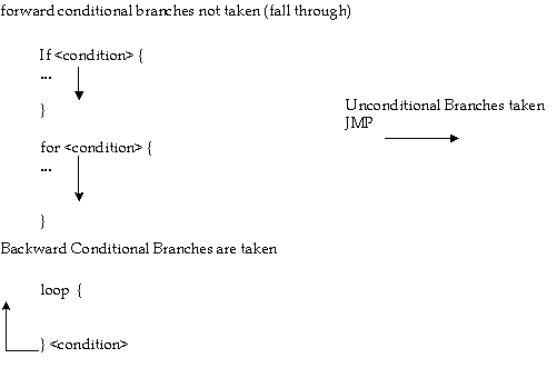
The following examples illustrate the basic rules for the static prediction algorithm.
A.Begin:	MOV	EAX, mem32
		AND	EAX, EBX
		IMUL	EAX, EDX
		SHLD	EAX, 7
		JC	Begin
In this example, the backwards (JC Begin) branch is not in the BTB the first time through, therefore, the BTB will not issue a prediction. The static predictor, however, will predict the branch to be taken, so a misprediction will not occur.
B.		MOV	EAX, mem32
		AND	EAX, EBX
		IMUL	EAX, EDX
		SHLD	EAX, 7
		JC	Begin
		MOV	EAX, 0
Begin:	Call 	Convert
The first branch instruction (JC Begin) in this code segment is a conditional forward branch. It is not in the BTB the first time through, but the static predictor will predict the branch to fall through.
The Call Convert instruction will not be predicted in the BTB the first time it is seen by the BTB, but the call will be predicted as taken by the static prediction algorithm. This is correct for an unconditional branch.
In these examples, the conditional branch has only two alternatives: taken and not taken. Indirect branches, such as switch statements, computed GOTOs or calls through pointers, can jump to an arbitrary number of locations. If the branch has a skewed target destination (that is, 90% of the time it branches to the same address), then the BTB will predict accurately most of the time. If, however, the target destination is not predictable, performance can degrade quickly. Performance can be improved by changing the indirect branches to conditional branches that can be predicted.
Scheduling or pairing should be done in a way that optimizes performance across all processor generations. The following is a list of pairing and scheduling rules that can improve the speed of your code on Pentium and P6-family processors. In some cases, there are tradeoffs involved in reaching optimal performance on a specific processor; these tradeoffs vary based on the specific characteristics of the application. On superscalar Pentium processors, the order of instructions is very important to achieving maximum performance.
Reordering instructions increases the possibility of issuing two instructions simultaneously. Instructions that have data dependencies should be separated by at least one other instruction.
This section describes the rules you need to follow to pair MMX instructions with integer instructions. For each of the conditions listed in the following table, the subsection lists the rules that apply.
Several types of rules must be observed to allow pairing:
Floating-point instructions are not pairable with MMX instructions.
For general pairing rules on Pentium processors, Optimizations for Intel's 32-bit Processors, Application Note AP-526, (Order Number 242816). The Pentium processors with MMX technology has relaxed some of the general pairing rules:
Pairing cannot be performed when the following two conditions occur:
3.3.2.1 Instructions that Cannot be Paired (NP)
Also see Section 3.3.2.2, No Pairing Allowed because of Register Dependencies.
3.3.2.2 Pairable Instructions Issued to U or V-pipes (UV)
3.3.2.3 Pairable Instructions Issued to U-pipe (PU)
3.3.2.4 Pairable Instructions Issued to V-pipe (PV)
These instructions can execute in either the U-pipe or the V-pipe but they are only paired when they are in the V-pipe. Since these instructions change the instruction pointer (eip), they cannot pair in the U-pipe since the next instruction may not be adjacent. Even when a branch in the U-pipe is predicted "not taken", the current instruction will not pair with the following instruction.
fxch
3.3.2.5 No Pairing Allowed Because of Register Dependencies
Instruction pairing is also affected by instruction operands. The following combinations cannot be paired because of register contention. Exceptions to these rules are given in the next section.
   mov  eax, 8
   mov  [ebp], eax
   mov  eax, 8
   mov  eax, [ebp]
This limitation does not apply to a pair of instructions which write to the EFLAGS register (for example, two ALU operations that change the condition codes). The condition code after the paired instructions execute will have the condition from the V-pipe instruction.
Note that two instructions in which the first reads a register and the second writes to a condition knowing it (anti-dependence) may be paired. See following example:
mov  eax, ebx
mov  ebx, [ebp]
For purposes of determining register contention, a reference to a byte or word register is treated as a reference to the entire 32-bit register. Therefore,
mov  al, 1
mov  ah, 0
do not pair due to output dependencies on the contents of the EAX register.
3.3.2.6 Special Pairs
There are some special instructions that can be paired in spite of our "general" rule above. These special pairs overcome register dependencies and most involve implicit reads/writes to the esp register or implicit writes to the condition codes.
Stack Pointer:
Condition Codes:
Note that special pairs that consist of PUSH/POP instructions may have only immediate or register operands, not memory operands.
3.3.2.7 Restrictions On Pair Execution
There are some pairs that may be issued simultaneously but will not execute in parallel. The following two rules must be followed to pair an MMX instruction in the U-pipe and an integer instruction in the V-pipe.
	add  eax, mem1
	add  ebx, mem2      ; 1
	(add)   (add)       ; 2  2-cycle
The instructions above add the contents of the register and the value at the memory location, then put the result in the register. An add with a memory operand takes two clocks to execute. The first clock loads the value from cache and the second clock performs the addition. Since there is only one memory access in the U-pipe instruction, the add in the V-pipe can start in the same cycle.
	add  meml, eax			; 1
	(add)				; 2
	(add)	add  mem2, ebx	; 3
	(add)				; 4
	(add)				; 5
The above instructions add the contents of the register to the memory location and store the result at the memory location. An add with a memory result takes three clocks to execute. The first clock loads the value, the second performs the addition and the third stores the result. When paired, the last cycle of the U-pipe instruction overlaps with the first cycle of the V-pipe instruction execution.
No other instructions may begin execution until the instructions already executing have completed.
To best expose opportunities for scheduling and pairing, it is better to issue a sequence of simple instructions rather than a complex instruction that takes the same number of cycles. The simple instruction sequence can take advantage of more issue slots. The load/store style code generation requires more registers and increases code size. To compensate for the extra registers needed, extra effort should be put into register allocation and instruction scheduling so that extra registers are used only when parallelism increases.
3.3.3.1 Pairing Two MMXTM Instructions:
3.3.3.2 Pairing an Integer Instruction in the U-Pipe with an MMXTM Instruction in the V-Pipe
3.3.3.4 Scheduling Rules
All MMX instructions may be pipelined including the multiply instructions. All instructions take a single clock to execute except MMX multiply instructions which take three clocks.
Since multiply instructions take three clocks to execute, the result of a multiply instruction can be used only by other instructions issued three clocks later. For this reason, avoid scheduling a dependent instruction in the two instruction pairs following the multiply.
As mentioned in Section 2.1.1, the store of a register after writing the register must wait for two clocks after the update of the register. Scheduling the store two clock cycles after the update avoids a pipeline stall.
The following section describes instruction selection optimizations.
An MMX instruction may have two register operands ("OP reg, reg") or one register and one memory operand ("OP reg, mem"), where OP represents the instruction operand and, reg represents the register and mem represents memory. "OP reg, mem" instructions are useful, in some cases, to reduce register pressure, increase the number of operations per cycle, and reduce code size.
The following discussion assumes that the memory operand is present in the data cache. If it is not, then the resulting penalty is usually large enough to obviate the scheduling effects discussed in this section.
In Pentium processors, "OP reg, mem" MMX instructions do not have longer latency than "OP reg, reg" instructions (assuming a cache hit). They do have more limited pairing opportunities, however (see Section 3.3.1). In dynamic execution (P6-family) processors, "OP reg, mem" MMX instructions translate into two micro-ops (as opposed to one uop for the "OP reg, reg" instructions). Thus, they tend to limit decoding bandwidth (see Section 2.1.2) and occupy more resources than "OP reg, reg" instructions.
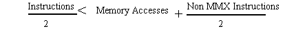
Recommended usage of "OP reg, mem" instructions depends on whether the MMX code is memory-bound (that is, execution speed is limited by memory accesses). As a rule of thumb, an MMX code section is considered to be memory-bound if the following inequality holds:
For memory-bound MMX code, Intel recommends to merge loads whenever the same memory address is used more than once. This reduces the number of memory accesses.
Example:
OP		MM0, [address A]
OP		MM1, [address A]
becomes:
MOVQ    	MM2, [address A]
OP     		MM0, MM2
OP      		MM1, MM2
For MMX code that is not memory-bound, load merging is recommended only if the same memory address is used more than twice. Where load merging is not possible, usage of "OP reg, mem" instructions is recommended to minimize instruction count and code size.
Example:
MOVQ		MM0, [address A]
OP		MM1, MM0
becomes:
OP MM1, [address A]
In many cases, a "MOVQ reg, reg" and "OP reg, mem" can be replaced by a "MOVQ reg, mem" and "OP reg, reg". This should be done where possible, since it saves one uop on dynamic execution processors.
Example: (here OP is a symmetric operation)
MOVQ		MM1, 	MM0			(1 micro-op)
OP		MM1, [address A]	(2 micro-ops)
becomes:
MOVQ    	MM1, [address A]	(1 micro-op)
OP      		MM1, MM0			(1 micro-op)
On Pentium processors, instructions greater than seven bytes in length cannot be executed in the V-pipe. In addition, two instructions cannot be pushed into the instruction FIFO (see Section 2.1.1) unless both are seven bytes or less in length. If only one instruction is pushed into the FIFO, pairing will not occur unless the FIFO already contains at least one instruction. In code where pairing is very high (this often happens in MMX code) or after a mispredicted branch, the FIFO may be empty, leading to a loss of pairing whenever the instruction length is over seven bytes.
In addition, dynamic execution (P6-family) processors can only decode one instruction at a time when an instruction is longer than seven bytes.
So, for best performance on all Intel processors, use simple instructions that are less than eight bytes in length (see Section 3.4.1 for one way to reduce instruction size).
Cache behavior can dramatically affect the performance of your application. By having a good understanding of how the cache works, you can structure your code to take best advantage of cache capabilities. For more information on the structure of the cache, see Section 2.2.
When a data access to a cacheable address misses the data cache, the entire cache line is brought into the cache from external memory. This is called a line fill. On Pentium and dynamic execution (P6-family) processors, these data arrive in a burst composed of four 8-byte sections in the following burst order:
Data are available for use in the order that they arrive from memory. If an array of data is being read serially, it is preferable to access it in sequential order so that each data item will be used as it arrives from memory.
Arrays with a size which is a multiple of 32 bytes should start at the beginning of a cache line. By aligning on a 32-byte boundary, you take advantage of the line fill ordering and match the cache line size. Arrays with sizes which are not multiples of 32 bytes should begin at 32- or 16-byte boundaries (the beginning or middle of a cache line). In order to align on a 16-or 32- byte boundary, you may need to pad the data. If this is necessary, try to locate data (variables or constants) in the padded space.
Dynamic execution (P6-family) processors have a "write allocate by read-for-ownership" cache, whereas the Pentium processor has a "no-write-allocate; write through on write miss" cache.
On dynamic execution (P6-family) processors, when a write occurs and the write misses the cache, the entire 32-byte cache line is fetched. On the Pentium processor, when the same write miss occurs, the write is simply sent out to memory.
Write allocate is generally advantageous, since sequential stores are merged into burst writes, and the data remains in the cache for use by later loads. This is why dynamic execution (P6-family) processors adopted this write strategy, and why some Pentium processor system designs implement it for the L2 cache, even though the Pentium processor uses write-through on a write miss.
Write allocate can be a disadvantage in code where:
When a large number of writes occur within an application, as in the example program below, and both the stride is longer than the 32-byte cache line and the array is large, every store on a dynamic execution (P6-family) processor will cause an entire cache line to be fetched. In addition, this fetch will probably replace one (sometimes two) dirty cache line.
The result is that every store causes an additional cache line fetch and slows down the execution of the program. When many writes occur in a program, the performance decrease can be significant. The Sieve of Erastothenes program is a simplistic example that demonstrates these cache effects. In this example, a large array is stepped through in increasing strides while writing a single value of the array with zero.
This is a very simplistic example used only to demonstrate cache effects; many other optimizations are possible in this code.
Sieve of Erastothenes example:
boolean array[2..max]
for(i=2;i<max;i++) {
     array := 1;
    }

for(i=2;i<max;i++) {
     if( array[i] ) {
         for(j=2;j<max;j+=i) {
          array[j] := 0;  /*here we assign memory to 0 causing 							the cache line
                        	fetch within the j loop */
         }
     }
}
Two optimizations are available for this specific example. One is to pack the array into bits, thereby reducing the size of the array, which in turn reduces the number of cache line fetches. The second is to check the value prior to writing, thereby reducing the number of writes to memory (dirty cache lines).
In the program above, 'Boolean' is a char array. It may well be better, in some programs, to make the "boolean" array into an array of bits, packed so that read-modify-writes are done (since the cache protocol makes every read into a read-modify-write). But, in this example, the vast majority of strides are greater than 256 bits (one cache line of bits), so the performance increase is not significant.
Another optimization is to check if the value is already zero before writing.
boolean array[2..max]
for(i=2;i<max;i++) {
     array := 1;
    }

    for(i=2;i<max;i++) {
     if( array[i] ) {
         for(j=2;j<max;j+=i) {
          if( array[j] != 0 ) {  /* check to see if value is 							already 0 */
              array[j] := 0;
          }
         }
     }
    }
The external bus activity is reduced by half because most of the time in the Sieve program the data is already zero. By checking first, you need only one burst bus cycle for the read and you save the burst bus cycle for every line you do not write. The actual write back of the modified line is no longer needed, therefore saving the extra cycles.
This operation benefits P6-family processors but may not enhance the performance of Pentium processors. As such, it should not be considered generic. Write allocate is generally a performance advantage in most systems, since sequential stores are merged into burst writes, and the data remain in the cache for use by later loads. This is why P6-family processors use this strategy, and why some Pentium processor-based systems implement it for the L2 cache.
The MMX registers allow you to move large quantities of data without stalling the processor. Instead of loading single array values that are 8-, 16-, or 32-bits long, consider loading the values in a single quadword, then incrementing the structure or array pointer accordingly.
Any data that will be manipulated by MMX instructions should be loaded using either;
All SIMD data should be stored using the MMX instruction that stores a 64-bit operand (for example, MOVQ m64, MM0).
The goal of these recommendations is twofold: First, the loading and storing of SIMD data is more efficient using the larger quadword data block sizes. Second, this helps to avoid the mixing of 8-, 16-, or 32-bit load and store operations with 64-bit MMX load and store operations to the same SIMD data. This, in turn, prevents situations in which a) small loads follow large stores to the same area of memory, or b) large loads follow small stores to the same area of memory. Dynamic execution processors will stall in these situations. (See list of rules in Section 3.1.1.).
Consider the following examples. In the first case, there is a large load after a series of small stores to the same area of memory (beginning at memory address "mem"). The large load will stall in this case:
        MOV     mem, eax		; store dword to address "mem"
        MOV     mem + 4, ebx		; store dword to address "mem + 4"
               :
               :
        MOVQ    mm0, mem		; load qword at address "mem", stalls
The MOVQ must wait for the stores to write memory before it can access all the data it requires. This stall can also occur with other data types (for example, when bytes or words are stored and then words or doublewords are read from the same area of memory). When you change the code sequence as follows, the processor can access the data without delay:
        MOVD	mm1, 	ebx		; build data into a qword first before
        				; storing it to memory
        MOVD	mm2,	eax
        PSLLQ	mm1,	32
        POR	mm1,	mm2
        MOVQ	mem,	mm1		; store SIMD variable to "mem" as a
					; qword
                :
                :
        MOVQ	mm0,	mem		; load qword SIMD variable "mem",no
					;stall
In the second case, there is a series of small loads after a large store to the same area of memory (beginning at memory address "mem"). The small loads will stall in this case:
        MOVQ    	mem,	mm0			; store qword to address
							; "mem"
                :
                :
        MOV     	bx,      	mem + 2  	; load word at address
							; "mem + 2", stalls
        MOV     	cx,      	mem + 4  	; load word at address
							; "mem + 4", stalls
The word loads must wait for the quadword store to write to memory before they can access the data they require. This stall can also occur with other data types (for example, when doublewords or words are stored and then words or bytes are read from the same area of memory). When you change the code sequence as follows, the processor can access the data without delay:
        MOVQ    	mem,	mm0      	; store qword to address "mem"
                :
                :
        MOVQ    	mm1,	mem      	; load qword at address "mem"
        MOVD    	eax,	mm1		; transfer "mem + 2" to ax from
						; MMX register not memory
        PSRLQ   	mm1, 	32
        SHR		eax,	16
        MOVD    	ebx,	mm1		; transfer "mem + 4" to bx from
						; MMX register, not memory
        AND	ebx, 	0ffffh
These transformations, in general, increase the number the instructions required to perform the desired operation. For dynamic execution (P6-family) processors, the performance penalty due to the increased number of instructions is more than offset by the benefit. For Pentium processors, however, the increased number of instructions can negatively impact performance, since they do not benefit from the code transformations above. For this reason, careful and efficient coding of these transformations is necessary to minimize any potential negative impact to Pentium processor performance.
It is beneficial to understand how memory is accessed and filled. A memory-to-memory fill (for example a memory-to-video fill) is defined as a 32-byte (cache line) load from memory which is immediately stored back to memory (such as a video frame buffer). The following are guidelines for obtaining higher bandwidth and shorter latencies for sequential memory fills (video fills). These recommendations are relevant for all Intel Architecture processors with MMX technology and refer to cases in which the loads and stores do not hit in the second level cache.
3.6.2.1 Memory Fills
3.6.2.1.1 Increasing Memory Bandwidth Using the MOVQ Instruction
Loading any value will cause an entire cache line to be loaded into the on-chip cache. But, using MOVQ to store the data back to memory instead of using 32-bit stores (for example, MOVD) will reduce by half the number of stores per memory fill cycle. As a result, the bandwidth of the memory fill cycle increases significantly. On some Pentium processor-based systems, 30% higher bandwidth was measured when 64-bit stores were used instead of 32-bit stores. Additionally, on dynamic execution processors, this avoids a partial memory access when both the loads and stores are done with the MOVQ instruction.
3.6.2.1.2 Increasing Memory Bandwidth by Loading and Storing To and From the Same DRAM Page
DRAM is divided into pages (which are not the same as Operating System (OS) pages. The size of a DRAM page is a function of the DRAM's size and organization. Page sizes of several Kbytes are common. Like OS pages, DRAM pages are constructed of sequential addresses. Sequential memory accesses to the same DRAM page have shorter latencies than sequential accesses to different DRAM pages. In many systems the latency for a page miss (that is, an access to a different page instead of the page previously accessed) can be twice as large as the latency of a memory page hit (access to the same page as the previous access). Therefore, if the loads and stores of the memory fill cycle are to the same DRAM page, we can see a significant increase in the bandwidth of the memory fill cycles.
3.6.2.1.3 Increasing the Memory Fill Bandwidth by Using Aligned Stores
Unaligned stores will double the number of stores to memory. Intel strongly recommends that quadword stores be 8-byte aligned. Four aligned quadword stores are required to write a cache line to memory. If the quadword store is not 8-byte aligned, then two 32 bit writes result from each MOVQ store instruction. On some systems, a 20% lower bandwidth was measured when 64 bit misaligned stores were used instead of aligned stores.
3.6.2.2 Video Fills
3.6.2.2.1 Use 64 Bit Stores to Increase the Bandwidth to Videob
Although the PCI bus between the processor and the Frame buffer is 32 bits wide, using MOVQ to store to video is faster on most Pentium processor-based systems than using twice as many 32-bit stores to video. This occurs because the bandwidth to PCI write buffers (which are located between the CPU and PCI bus) is higher when quadword stores are used.
3.6.2.2.2 Increase the Bandwidth to Video Using Aligned Stores
When a non-aligned store is encountered, there is a dramatic decrease in the bandwidth to video. Misalignment causes twice as many stores, and, in addition, the latency of stores on the PCI bus (to the Frame buffer) is much longer. On the PCI bus, it is not possible to burst sequential misaligned stores. On Pentium processor-based systems, a decrease of 80% in the video fill bandwidth is typical when misaligned stores are used instead of aligned stores.
Legal Stuff © 1997 Intel Corporation
