
Chapter 2
OVERVIEW OF PROCESSOR ARCHITECTURE AND PIPELINES
The Pentium processor is an advanced superscalar processor. It is built around two general-purpose integer pipelines and a pipelined floating-point unit, allowing the processor to execute two integer instructions simultaneously. A software-transparent dynamic branch-prediction mechanism minimizes pipeline stalls due to branches. Pentium processors with MMX technology add additional stages to the pipeline. The integration of the MMX Technology pipeline with the integer pipeline is very similar to that of the floating-point pipe.
Pentium processors can issue two instructions every clock cycle, one in each pipe. The first logical pipe is referred to as the "U" pipe, and the second as the "V" pipe. During decoding of any given instruction, the next two instructions are checked, and, if possible, they are issued such that the first one executes in the U-pipe and the second in the V-pipe. If it is not possible to issue two instructions, then the next instruction is issued to the U-pipe and no instruction is issued to the V-pipe.
When instructions execute in the two pipes, their
behavior is exactly the same as if they were executed sequentially.
When a stall occurs, successive instructions are not allowed to
pass the stalled instruction in either pipe.
Figure 2-1 shows the pipelining structure
for this scheme:

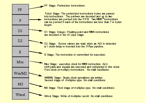
Pentium processors with MMX technology add an additional stage to the integer pipeline. The instruction bytes are prefetched from the code cache in the prefetch (PF) stage, and they are parsed into instructions in the fetch (F) stage. Additionally, any prefixes are decoded in the F stage.
Instruction parsing is decoupled from the instruction decoding by means of an instruction First In, First Out (FIFO) buffer, which is situated between the F and Decode 1 (D1) stages. The FIFO has slots for up to four instructions. This FIFO is transparent; it does not add additional latency when it is empty.
During every clock cycle, two instructions can be pushed into the instruction FIFO (depending on availability of the code bytes, and on other factors such as prefixes). Instruction pairs are pulled out of the FIFO into the D1 stage. Since the average rate of instruction execution is less than two per clock, the FIFO is normally full. As long as the FIFO is full, it can buffer any stalls that may occur during instruction fetch and parsing. If such a stall occurs, the FIFO prevents the stall from causing a stall in the execution stage of the pipe. If the FIFO is empty, then an execution stall may result from the pipeline being "starved" for instructions to execute. Stalls at the FIFO entrance may result from long instructions or prefixes (see Sections 3.2.3 and 3.4.2).
The following chart details the MMX technology pipeline on superscalar
processors and the conditions in which a stall may occur in the
pipeline.

Table 2-1 details the functional units, latency, throughput, and execution pipes for each type of MMX technology instruction.
Functional Units | Pipes | |||
Information on pairing requirements can be found in Section 3.3.
Additional information on instruction format can be found in the Intel Architecture MMXTM Technology Programmer's Reference Manual, (Order Number 243007).
P6-family processors use a Dynamic Execution architecture that
blend out-of-order and speculative execution with
hardware register renaming and branch prediction. These processors
feature an in-order issue pipeline, which breaks Intel386TM
processor macroinstructions up into simple, micro-operations called
micro-ops (or uops), and an out-of-order, superscalar processor
core, which executes the micro-ops. The out-of-order core of the
processor contains several pipelines to which integer, jump, floating-point,
and memory execution units are attached. Several different execution
units may be clustered on the same pipeline: for example, an integer
address logic unit and the floating-point execution units (adder,
multiplier, and divider) share a pipeline. The data cache is pseudo-dual
ported via interleaving, with one port dedicated to loads and
the other to stores. Most simple operations (integer ALU, floating-point
add, even floating-point multiply) can be pipelined with a throughput
of one or two operations per clock cycle. Floating-point divide
is not pipelined. Long latency operations can proceed in parallel
with short latency operations.
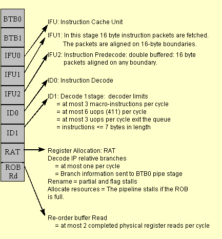
The P6-family pipeline is comprised of three parts: the In-Order
Issue Front-end, the Out-of-Order Core and the In-Order Retirement
unit. Details about the In-Order Issue Front-end follow below.

Since the dynamic execution processors execute instructions out of order, the most important consideration in performance tuning is making sure enough micro-ops are ready for execution. Correct branch prediction and fast decoding are essential to getting the most performance out of the In-Order Front-End. Branch prediction and the branch target buffer are detailed in Section 2.3. Decoding is discussed below.
During every clock cycle, up to three Intel Architecture macro instructions can be decoded in the ID1 pipestage. However, if the instructions are complex or are over seven bytes then the decoder is limited to decoding fewer instructions.
The decoders can decode:
P6-family processors have three decoders in the D1 pipestage. The first decoder is capable of decoding one IA macro-instruction of four or fewer micro-ops in each clock cycle. The other two decoders can each decode an IA instruction of one micro-op in each clock cycle. Instructions composed of more than four micro-ops will take multiple cycles to decode. When programming in assembly language, scheduling the instructions in a 4-1-1 micro-op sequence increases the number of instructions that can be decoded each clock cycle. In general:
For the purpose of counting micro-ops, MMX technology instructions are simple instructions. See Optimizations for Intel's 32-bit Processors, Application Note AP-526 (Order Number 242816), Appendix D for a table that specifies the number of micro-ops for each instruction in the Intel Architecture instruction set.
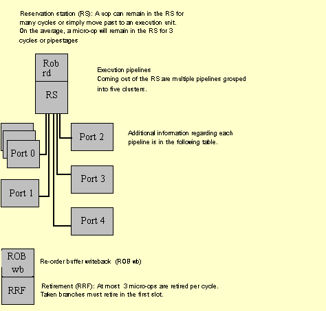
Once the micro-ops are decoded, they will be issued from the In-Order Front-End into the Reservation Station (RS), which is the beginning pipestage of the Out-of-Order core. In the RS, the micro-ops wait until their data operands are available. Once a micro-op has all data sources available, it will be dispatched from the RS to an execution unit. If a micro-op enters the RS in a data-ready state (that is, all data is available), then the micro-op will be immediately dispatched to an appropriate execution unit, if one is available. In this case, the micro-op will spend very few clock cycles in the RS. All of the execution units are clustered on ports coming out of the RS. Once the micro-op has been executed it returns to the ROB, and waits for retirement. In this pipestage, all data values are written back to memory and all micro-ops are retired in-order, three at a time. The figure below provides details about the Out-of-Order core and the In-Order retirement pipestages.

| ||
| Integer ALU Unit
LEA instructions Shift instructions Integer Multiplication instruction
Floating-Point Unit MMXTM Technology ALU Unit MMX Technology Multiplier UnitFDIV | Latency 1, Thruput 1/cycle
Latency 1, Thruput 1/cycle Latency 1, Thruput 1/cycle
Latency 4, Thruput 1/cycle
Latency 3, Thruput 1/cycle Latency 1, Thruput1/cycle Latency 3, Thruput 1/cycle | |
| Integer ALU Unit
MMX Technology ALU Unit MMX Technology Shifter Unit | Latency 1, Thruput 1/cycle
Latency 1, Thruput 1/cycle Latency 1, Thruput 1/cycle | |
| Load Unit | Latency 3 on a cache hit,
Thruput 1/cycle4 | |
| Store Address Unit | Latency 3 (not applicable)
Thruput 1/cycle3 | |
| Store Data Unit | Latency 1 (not applicable)
Thruput 1/cycle | |
Notes:
The on-chip cache subsystem of processors with MMX technology consists of two 16 K four-way set associative caches with a cache line length of 32 bytes. The caches employ a write-back mechanism and a pseudo-LRU replacement algorithm. The data cache consists of eight banks interleaved on four-byte boundaries.
On Pentium processors with MMX technology, the data cache can be accessed simultaneously from both pipes, as long as the references are to different cache banks. On the dynamic execution (P6-family) processors, the data cache can be accessed simultaneously by a load instruction and a store instruction, as long as the references are to different cache banks. The delay for a cache miss on the Pentium processor with MMX technology is eight internal clock cycles. On dynamic execution processors with MMX technology the minimum delay is ten internal clock cycles.
Branch prediction for Pentium and dynamic execution processors with MMX technology is functionally identical except for one minor exception which will be discussed in Section 2.3.1.
The Branch Target Buffer (BTB) stores the history of the previously seen branches and their targets. When a branch is prefetched, the BTB feeds the target address directly into the Instruction Fetch Unit (IFU). Once the branch is executed, the BTB is updated with the target address. Using the branch target buffer, branches that have been seen previously are dynamically predicted. The branch target buffer prediction algorithm includes pattern matching and up to four prediction history bits per target address. For example, a loop which is four iterations long should have close to 100% correct prediction. Adhering to the following guideline will improve branch prediction performance:
Program conditional branches (except for loops) so that the most executed branch immediately follows the branch instruction (that is, fall through).
Additionally, processors with MMX technology have a Return Stack Buffer (RSB), which can correctly predict return addresses for procedures that are called from different locations in succession. This increases further the benefit of unrolling loops which contain function calls, and removes the need to in-line certain procedures.
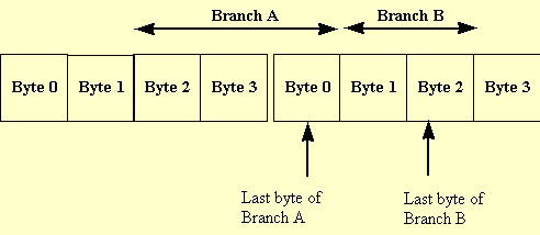
On the Pentium processor with MMX technology, branches may be mispredicted when the last byte of two branch instructions occur in the same aligned four byte section of memory, as shown in the figure below.

This may occur when there are two consecutive branches with no intervening instructions and the second instruction is only two bytes long (such as a jump relative +/- 128).
To avoid a misprediction in these cases, make the second branch longer by using a 16-bit relative displacement on the branch instruction instead of an 8-bit relative displacement.
Processors with MMX technology have four write buffers (versus two in Pentium processors without MMX technology). Additionally, the write buffers can be used by either the U-pipe or the V-pipe (versus one corresponding to each pipe in Pentium processors without MMX technology). Performance of critical loops can be improved by scheduling the writes to memory; when you expect to see write misses, you should schedule the write instructions in groups no larger than four, then schedule other instructions before scheduling further write instructions.
Legal Stuff © 1997 Intel Corporation