What You'll Find Inside
The SmartDie product specification documents contain die-level information about individual SmartDie products. They are not meant to duplicate data that is readily available in other Intel documents such as the packaged product data sheets.
Each product specification consists of feature bullets, a die photo, die plot, pad coordinate table, SmartDie product processing description, special handling instructions (when appropriate), physical specifications, D/C specifications, ordering information, reference documents, and a document revision history. Listed below are descriptions of the SmartDie Product Specifications sections.
Note that die specifications may change more frequently than our packaged product data sheets. This is because die topography changes often do not affect the package footprint and are therefore transparent to users. For this reason, we highly recommend that you contact your local Intel Sales Office to verify that you have the latest SmartDie product specification before finalizing your design.
For More Information
If, after reading this specification document, you would still like more information, please call the appropriate Intel FaxBack number:
Intel Literature Department 1-800-548-4725
Intel FAXBACK (U.S. or Canada) 1-800-628-2283 or 1-916-356-3105
Intel FAXBACK (Europe) 44(0)793-496646
Section Descriptions
Feature Bullets
Feature bullets highlight the precise versions of the SmartDie product and key architectural and performance features. You'll also find here the die junction temperature range (average silicon surface temperature) rather than the Tc (case temperature) range, which is commonly provided for our packaged products.
Die Photograph
A photograph of the SmartDie product is provided to show key topographical features and to demonstrate proper shipping orientation within shipping media. The photo might also be useful for confirming product orientation at incoming inspection prior to use within automatic insertion equipment. You might find it useful to create a mockup of your design using the photo to indicate die position and orientation.
Pad Passivation Opening Plot
The active (top) surfaces of all SmartDie products have a protective coating called a passivation layer which protects the die from scratches and ionic contamination during handling. The composition and thickness of this layer are detailed in the physical specification section. In this passivation layer is a pattern of openings for the bonding pads for signal and power supply connectivity. The product specification includes plots of these functional die pad openings to assist with design.
These pads are numbered to allow you to identify specific pads simply by counting in from the corner locations. Because of their small size and to avoid clutter, only the numbers of pad 1 and the corner pads are typically shown. Pad names are listed separately in a Bond Pad Center Data Table. Intel numbers the pads counter-clockwise starting with pad 1, using a top-die view. Even "No Connect" (NC) pads are numbered.
Each passivation plot has a GEL-PAK notch indicator. The plot and photo are both oriented relative to the notch in the same way the die is shipped, which allows you to use automated pick-and-place equipment in manufacturing.
X/Y reference directions are also indicated on all plots. They're valid for the bond pad center coordinates as well as for the die dimensions.
You'll also notice an enlarged version of the die logo, along with copyright information, in a circle. A line leads to a smaller circle containing the same information. The smaller circle indicates the relative position of this information as it appears on the die. With the aid of a microscope you can use it as a secondary confirmation of die orientation.
Many plots contain irregular shapes on two or more corners to indicate the shape and location of fiducials on the die. Because fiducials are not bond pads, they must not have electrical connectivity. They are used by Intel manufacturing to align mask layers, but they may also be useful to you in optimizing wirebond placements for wire-bonders that have pattern recognition capability.
Plots are intended to be scaled versions of the pad passivation openings. You can use the irregular placement of pads on some SmartDie products to locate specific pads. For example, it is easier to locate the third pad from an irregularly spaced pad than to count 46 pads from a numbered corner pad.
Bond Pad Center Data
Bond pad center data provides the relative positions of the functional die pads and their signal names. Values are listed in both mils (thousandths of an inch or 25.400 microns) and microns (millionths of a meter). All dimensions are referenced from the center of the die and define the center of the bond pad passivation opening. See Figure 1 below which has an example of the bond pad center data for pad #25 (See Table 1) on the Intel 486SX.
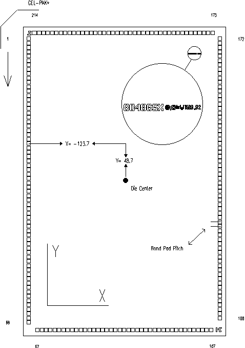
Figure 1 : Intel486 SX Microprocessor Die/Bond Pad Layout
Table 1 is an example of the Bond Pad Center Data Table for the Intel486 SX Microprocessor. This example shows the data for pads 20-25.
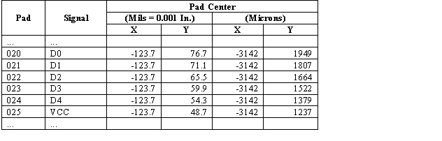
Table 1 Bond Pad Center Data
Although coordinates for the corners of passivation openings are not listed, they can be calculated using the center coordinates and the passivation opening dimensions listed in the physical specifications. For pads which are non-symmetrical (example: 3 mil x 5 mil), we show individual pad orientations on the passivation opening plot. The X/Y orientation shown on the passivation opening plot is used for all pad coordinates.
A note section follows the bond pad center data table identifying pads with irregular shapes (ex: double-wide), NC (No Connect) pads, usage of the "#" sign to identify active low signals, and any other information deemed useful to users of SmartDie products.
Intel SmartDie Product Processing
This section of the product specification details the various processes SmartDie products undergo. These include testing, wafer sawing, die separation, die placement in shipping media, visual inspections, packing, labeling, storage requirements, and ESD sensitivity.
Specifications
Post-saw die dimensions
Intel provides die length, width, and height (thickness) in mil units; length and width are reported using the same X/Y reference directions shown on the passivation opening plot. (Example: X = 450 +/- 0.5, Y = 416 +/- 0.5.) X/Y dimensions are reported as post-saw, since a thin slice of silicon is cut away during each saw swath. All dimensions list tolerance values to account for process variations. See Figure 2 for an example.
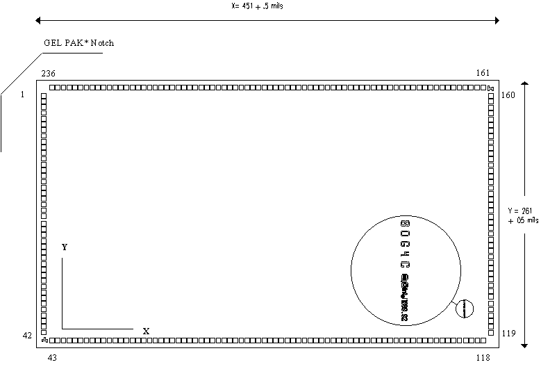
Figure 2 : Post-Saw Die Dimensions for Intel 486 DX2
Die backside metalization
Intel's most common variations of wafer backside metalization are gold/chrome and polished bare silicon. In both, we perform backlapping on each wafer. Backlapping removes contaminants (typically from wafer process diffusion steps) and native oxides, and planarizes the back surface of the wafer to reduce potential voiding in the die-attach material. In the case of gold/chrome backsides, backlapping is performed prior to the deposition of these layers. Because they are so thin, backside metalization layers are typically reported in Angstroms. (10,000 Angstroms equal one micron.)
Gold/Chrome
The die backside consists of a layer of gold (typical thickness - 1500 Angstroms) over a layer of chrome (150 Angstroms). Gold provides high reliability for eutectic die attach and good ohmic contact for adhesive paste die attachments. Chrome acts as a diffusion barrier layer to prevent surface oxidation at storage temperatures and allows rapid silicon diffusion to occur at eutectic die attach temperatures.
Polished bare silicon
A polished bare silicon backside consists of pure silicon. It is commonly used for die products that do not require a 'driven' electrical backside bias. SmartDie product specifications state whether backside biasing must be driven or whether float is acceptable.
Pad passivation opening size
The dimensions of the pad openings are reported in both mils and microns. We also provide the dimensions of any non-standard sized pad openings, identified in the Bond Pad Center Data table. Non-standard pads sometimes have unique wirebond recommendations.
Pad pitch
The term pitch is the center-to-center 'repeat' distance of equal sized objects placed in a row. Pitch can be measured from different reference points, (i.e. lower right corner to lower right corner), but the emphasis is on the term 'repeat'. Whether measured center-to-center or right corner to right corner, the distance is the same. Minimum pitch is a consideration for selection of wire bonding equipment and if bumps are to be grown on the bond pads or deposited for flip chip applications. See Figure 1 for an illustration of bond pad pitch.
Some Intel SmartDie products have uniform pad pitch on any one die side. For dies with varying pad pitches, Intel identifies the location of minimum value with a note referencing the two pads and the pitch value.
DC Specifications
Absolute Maximum Ratings (Die and Gel-Pak)
Stressing a die or Gel-Pak beyond the absolute maximum rating may cause permanent damage. Absolute maximum ratings are listed for the following categories:
Operating Conditions
Operating conditions include power supply voltage and tolerance, operating frequencies, and junction temperature under bias (Tj). Tj is defined as the average temperature of the active silicon die surface at any instant.
Substrate bias requirements
(Note: this information appears in the physical specification section of older SmartDie product specifications.) Most Intel SmartDie products require a backside electrical bias connection to either VCC or Vss, as stated in the die specification. Intel Flash SmartDie products are an exception in that you may float the die backside during operation without performance degradation. The specific substrate requirements of each SmartDie product are provided in this section.
Device nomenclature
Ordering information is provided here, including all valid variations of access time, supply voltage and clock frequency available. All SmartDie products begin with a package designator of "X".
Reference information
Order numbers for related Intel documents are listed in this section.
Revision history
All SmartDie product specification revisions are listed with a description of the changes made.
Legal Stuff © 1997 Intel Corporation
