Features
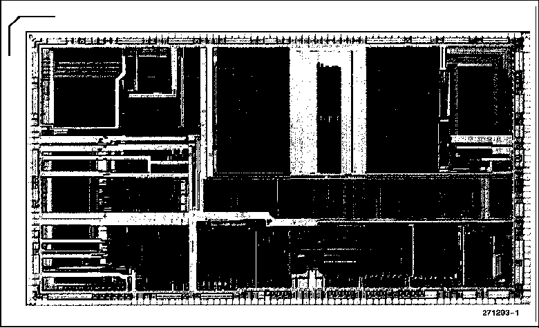
Intel 486 DX2 Microprocessor Die Photo
Die Specifications
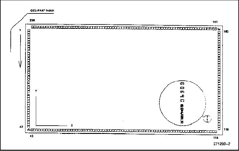
Table 1 Intel 486 DX2 Microprocessor Bond Pad Center Data
2.0 Intel Die Products Processing
Wafer Probe
Wafer Saw
Die Inspection
Packing Procedure
Inspection Steps
Storage Requirements
ESD
3.0 Specifications
3.1 Physical Specifications
3.2 DC Specifications
Absolute Maximum Ratings*
Operating Conditions*
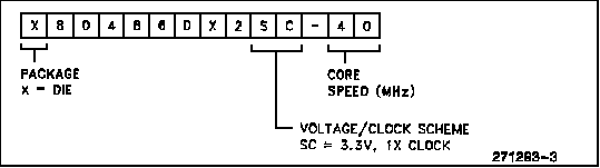
4.0 Device Nomenclature
5.0 Reference Information
6.0 Revision History
|
|
Notice: This document contains preliminary information on new products in production. It is valid for the devices indicated in the revision history. This specification is subject to change without notice. Verify with your local Intel Sales Office that you have the latest Smartdie product specification before finalizing a design.
Reference Information: The information in this document is provided as a supplement to the Standard Package Data Sheet on a specific product. Please reference the Standard Package Data Sheet (Order No. 242202) for additional product information and specifications not found in this document.
| Pad | Signal | Pad Center | |||
| (Mils 0.001 in.) | (Microns) | ||||
| X | Y | X | Y | ||
| 001 | V00 | -218.6 | 115.9 | -5553 | 2945 |
| 002 | V35 | -218.6 | 110.3 | -5553 | 2802 |
| 003 | D21 | -218.6 | 104.7 | -5553 | 2660 |
| 004 | D22 | -218.6 | 99.1 | -5553 | 2517 |
| 005 | D23 | -218.6 | 93.5 | -5553 | 2375 |
| 006 | DP3 | -218.6 | 87.9 | -5553 | 2232 |
| 007 | V00 | -218.6 | 82.3 | -5553 | 2090 |
| 008 | V55 | -218.6 | 76.7 | -5553 | 1947 |
| 009 | D24 | -218.6 | 71.1 | -5553 | 1805 |
| 010 | D25 | -218.6 | 65.5 | -5553 | 1662 |
| 011 | D26 | -218.6 | 59.8 | -5553 | 1520 |
| 012 | D27 | -218.6 | 54.2 | -5553 | 1377 |
| 013 | VCC | -218.6 | 48.6 | -5553 | 1235 |
| 014 | VSS | -218.6 | 43.0 | -5553 | 1092 |
| 015 | V00 | -218.6 | 37.4 | -5553 | 950 |
| 016 | V85 | -216.6 | 31.8 | -5553 | 607 |
| 017 | V00 | -218.6 | 26.2 | -5553 | 665 |
| 018 | V85 | -216.6 | 20.6 | -5553 | 522 |
| 019 | 028 | -218.6 | 15.0 | -5553 | 380 |
| 020 | D29 | -218.6 | 9.4 | -5553 | 237 |
| 021 | D30 | -218.6 | 3.7 | -5553 | 95 |
| 022 | D31 | -218.6 | -1.9 | -5553 | -47 |
| 023 | STPCLK# | -218.6 | -9.4 | -5553 | -237 |
| 024 | IGNNE# | -218.6 | -15.0 | -5553 | -380 |
| 025 | TOO | -218.6 | -20.6 | -5553 | -522 |
| 026 | FERR# | -218.6 | -26.2 | -5553 | -665 |
| 027 | SMI# | -218.6 | -31.8 | -5553 | -807 |
| 028 | V00 | -218.6 | -37.4 | -5553 | -950 |
| 029 | V35 | -218.6 | -43.0 | -5553 | -1092 |
| 030 | V00 | -218.6 | -48.6 | -5553 | -1235 |
| 031 | V88 | -218.6 | -54.2 | -5553 | -1377 |
| 032 | V00 | -218.6 | -59.8 | -5553 | -1520 |
| 033 | V88 | -218.6 | -65.5 | -5553 | -1662 |
| 034 | SMIAGT# | -218.6 | -71.1 | -5553 | -1805 |
| 035 | SRESET | -218.6 | -76.7 | -5553 | -1947 |
| 036 | N.C. | -218.6 | -82.3 | -5553 | -2090 |
| 037 | N.C. | -218.6 | -87.9 | -5553 | -2232 |
| 038 | N.C. | -218.6 | -93.5 | -5553 | -2375 |
| 039 | VCC | -218.6 | -99.1 | -5553 | -2517 |
| 040 | VSS | -218.6 | -104.7 | -5553 | -2660 |
| 041 | VSS | -218.8 | -110.3 | -5553 | -2802 |
| 042 | VCC | -218.6 | -115.9 | -5553 | -2945 |
| 043 | VCC | -210.9 | -123.7 | -5356 | -3142 |
| 044 | VSS | -205.2 | -123.7 | -5213 | -3142 |
| 045 | N.C. | -199.6 | -123.7 | -5071 | -3142 |
| 046 | N.C. | -194.0 | -123.7 | -4928 | -3142 |
| 047 | N.C. | -188.4 | -123.7 | -4786 | -3142 |
| 048 | N.C. | -182.8 | -123.7 | -4643 | -3142 |
| 049 | N.C. | -177.2 | -123.7 | -4501 | -3142 |
| 050 | N.C. | -171.6 | -123.7 | -4358 | -3142 |
| 051 | N.C. | -166.0 | -123.7 | -4216 | -3142 |
| 052 | NMI | -160.4 | -123.7 | -4073 | -3142 |
| 053 | INTR | -154.7 | -123.7 | -3931 | -3142 |
| 054 | FLUSH# | -149.1 | -123.7 | -3788 | -3142 |
| 055 | RESET | -143.5 | -123.7 | -3648 | -3142 |
| 056 | A20M# | -137.9 | -123.7 | -3503 | -3142 |
| 057 | EADS# | -132.3 | -123.7 | -3361 | -3142 |
| 058 | VSS | -126.7 | -123.7 | -3218 | -3142 |
| 059 | VCC | -121.1 | -123.7 | -3076 | -3142 |
| 060 | VSS | -115.5 | -123.7 | -2933 | -3142 |
| 061 | VCC | -109.9 | -123.7 | -2791 | -3142 |
| 062 | PCD | -104.3 | -123.7 | -2648 | -3142 |
| 063 | PWT | -98.6 | -123.7 | -2506 | -3142 |
| 084 | D/C# | -93.0 | -123.7 | -2363 | -3142 |
| 065 | M/IO# | -87.4 | -123.7 | -2221 | -3142 |
| 066 | VSS | -81.8 | -123.7 | -2078 | -3142 |
| 087 | VSS | -76.2 | -123.7 | -1936 | -3142 |
| 068 | VCC | -70.6 | -123.7 | -1793 | -3142 |
| 069 | BE3# | -65.0 | -123.7 | -1651 | -3142 |
| 070 | BE2# | -59.4 | -123.7 | -1508 | -3142 |
| 071 | SE1# | -53.8 | -123.7 | -1366 | -3142 |
| 072 | 13E0# | -48.2 | -123.7 | -1223 | -3142 |
| 073 | BREC | -42.5 | -123.7 | -1081 | -3142 |
| 074 | VSS | -36.9 | -123.7 | -938 | -3142 |
| 075 | VCC | -31.3 | -123.7 | -796 | -3142 |
| 076 | VSS | -25.7 | -123.7 | -653 | -3142 |
| 077 | VCC | -20.1 | -123.7 | -511 | -3142 |
| 078 | W/R# | -14.5 | -123.7 | -368 | -3142 |
| 079 | HILDA | -8.9 | -123.7 | -226 | -3142 |
| 050 | CLK | -3.3 | -123.7 | -83 | -3142 |
| 081 | N.C. | 2.3 | -123.7 | 59 | -3142 |
| 082 | VCC | 7.9 | -123.7 | 202 | -3142 |
| 083 | VSS | 13.6 | -123.7 | 344 | -3142 |
| 084 | VCC | 19.2 | -123.7 | 487 | -3142 |
| 085 | VSS | 24.8 | -123.7 | 629 | -3142 |
| 086 | VCC | 30.4 | -123.7 | 772 | -3142 |
| 087 | VSS | 36.0 | -123.7 | 914 | -3142 |
| 058 | VCC | 41.6 | -123.7 | 1057 | -3142 |
| 089 | N.C. | 47.2 | -123.7 | 1199 | -3142 |
| 090 | TCK | 52.8 | -123.7 | 1342 | -3142 |
| 091 | AHOLD | 58.4 | -123.7 | 1484 | -3142 |
| 092 | HOLD | 64.1 | -123.7 | 1627 | -3142 |
| 093 | VSS | 69.7 | -123.7 | 1769 | -3142 |
| 094 | VCC | 75.3 | -123.7 | 1912 | -3142 |
| 095 | KEN# | 80.9 | -123.7 | 2054 | -3142 |
| 098 | RDY# | 86.5 | -123.7 | 2197 | -3142 |
| 097 | NC. | 92.1 | -123.7 | 2339 | -3142 |
| 098 | VSS | 97.7 | -123.7 | 2482 | -3142 |
| 099 | VCC | 103.3 | -123.7 | 2624 | -3142 |
| 100 | BS8# | 108.9 | -123.7 | 2767 | -3142 |
| 101 | BS16# | 114.5 | -123.7 | 2909 | -3142 |
| 102 | BOFF# | 120.2 | -123.7 | 3052 | -3142 |
| 103 | BRDY# | 125.8 | -123.7 | 3194 | -3142 |
| 104 | PCHK# | 131.4 | -123.7 | 3337 | -3142 |
| 105 | N.C. | 137.0 | -123.7 | 3479 | -3142 |
| 106 | VSS | 142.8 | -123.7 | 3622 | -3142 |
| 107 | VCC | 148.2 | -123.7 | 3764 | -3142 |
| 108 | V SS | 153.8 | -123.7 | 3907 | -3142 |
| 109 | V00 | 159.4 | -123.7 | 4049 | -3142 |
| 110 | LOCK# | 165.0 | -123.7 | 4192 | -3142 |
| 111 | PLOGK# | 170.6 | -123.7 | 4334 | -3142 |
| 112 | VSS | 176.3 | -123.7 | 4477 | -3142 |
| 113 | VCC | 181.9 | -123.7 | 4619 | -3142 |
| 114 | BLAST# | 187.5 | -123.7 | 4762 | -3142 |
| 115 | ADS# | 194.0 | -123.7 | 4928 | -3142 |
| 116 | A2 | 199.6 | -123.7 | 5071 | -3142 |
| 117 | VSS | 205.2 | -123.7 | 5213 | -3142 |
| 118 | VCC | 210.9 | 123.7 | 5356 | -3142 |
| 119 | VCC | 218.6 | -116.2 | 5553 | -2953 |
| 120 | VSS | 218.6 | -110.3 | 5553 | -2802 |
| 121 | A3 | 218.6 | -104.7 | 5553 | -2660 |
| 122 | A4 | 218.6 | -99.1 | 5553 | -2517 |
| 123 | A5 | 218.6 | -93.5 | 5553 | -2375 |
| 124 | UP# | 218.6 | -87.9 | 5553. | -2232 |
| 125 | A6 | 218.6 | -81.0 | 5553 | -2057 |
| 126 | A7 | 218.6 | -75.4 | 5553 | -1914 |
| 127 | A8 | 218.6 | -69.8 | 5553 | -1772 |
| 128 | VSS | 218.6 | -64.1 | 5553 | -1629 |
| 129 | VCC | 218.6 | -58.5 | 5553 | -1487 |
| 130 | VSS | 218.6 | -52.9 | 5553 | -1344 |
| 131 | VCC | 218.6 | -47.3 | 5553 | -1202 |
| 132 | A9 | 218.6 | -41.7 | 5553 | -1059 |
| 133 | A10 | 218.6 | -36.1 | 5553 | -917 |
| 134 | VSS | 218.6 | -30.5 | 5553 | -774 |
| 135 | VCC | 218.6 | -24.9 | 5553 | -632 |
| 136 | VSS | 218.6 | -19.3 | 5553 | -489 |
| 137 | VCC | 218.6 | -13.7 | 5553 | -347 |
| 138 | VSS | 218.8 | -8.0 | 5553 | -204 |
| 139 | VCC | 218.6 | -2.4 | 5553 | -62 |
| 140 | A11 | 218.6 | 3.2 | 5553 | 81 |
| 141 | N.C. | 218.6 | 8.8 | 5553 | 223 |
| 142 | A12 | 218.6 | 14.4 | 5553 | 366 |
| 143 | VSS | 218.6 | 20.0 | 5553 | 508 |
| 144 | VCC | 218.8 | 25.6 | 5553 | 651 |
| 145 | A13 | 218.6 | 31.2 | 5553 | 793 |
| 146 | A14 | 218.5 | 36.8 | 5553 | 936 |
| 147 | VSS | 218.6 | 42.5 | 5553 | 1078 |
| 148 | VCC | 218.6 | 48.1 | 5553 | 1221 |
| 149 | A15 | 218.6 | 53.7 | 5553 | 1363 |
| 150 | A16 | 218.6 | 59.3 | 5553 | 1506 |
| 151 | A17 | 218.6 | 64.9 | 5553 | 1645 |
| 152 | VSS | 218.6 | 70.5 | 5553 | 1791 |
| 153 | VCC | 218.6 | 76.1 | 5553 | 1933 |
| 154 | TID | 218.6 | 81.7 | 5553 | 2076 |
| 155 | TMS | 218.6 | 87.3 | 5553 | 2218 |
| 156 | A18 | 218.6 | 92.9 | 5553 | 2361 |
| 157 | A19 | 218.6 | 98.6 | 5553 | 2503 |
| 158 | A20 | 218.6 | 104.2 | 5553 | 2646 |
| 159 | VSS | 218.6 | 110.3 | 5553 | 2802 |
| 160 | VCC | 218.6 | 115.9 | 5553 | 2945 |
| 161 | VCC | 210.9 | 123.7 | 5356 | 3142 |
| 162 | VSS | 204.9 | 123.7 | 5206 | 3142 |
| 163 | A21 | 198.7 | 123.7 | 5047 | 3142 |
| 164 | A22 | 193.1 | 123.7 | 4904 | 3142 |
| 165 | A23 | 187.5 | 123.7 | 4762 | 3142 |
| 166 | A24 | 181.9 | 123.7 | 4619 | 3142 |
| 167 | VCC | 176.3 | 123.7 | 4477 | 3142 |
| 168 | VSS | 170.6 | 123.7 | 4334 | 3142 |
| 169 | A25 | 165.0 | 123.7 | 4192 | 3142 |
| 170 | A26 | 159.4 | 123.7 | 4049 | 3142 |
| 171 | A27 | 153.8 | 123.7 | 3907 | 3142 |
| 172 | A28 | 148.2 | 123.7 | 3764 | 3142 |
| 173 | VCC | 142.6 | 123.7 | 3622 | 3142 |
| 174 | VSS | 137.0 | 123.7 | 3479 | 3142 |
| 175 | A29 | 131.4 | 123.7 | 3337 | 3142 |
| 176 | A30 | 125.8 | 123.7 | 3194 | 3142 |
| 177 | A31 | 120.2 | 123.7 | 3052 | 3142 |
| 178 | N.C. | 114.5 | 123.7 | 2909 | 3142 |
| 179 | DP0 | 108.9 | 123.7 | 2767 | 3142 |
| 180 | D0 | 103.3 | 123.7 | 2624 | 3142 |
| 181 | Dl | 97.7 | 123.7 | 2482 | 3142 |
| 182 | D2 | 92.1 | 123.7 | 2339 | 3142 |
| 183 | D3 | 86.5 | 123.7 | 2197 | 3142 |
| 184 | D4 | 80.9 | 123.7 | 2054 | 3142 |
| 185 | VCC | 75.3 | 123.7 | 1912 | 3142 |
| 186 | VSS | 69.7 | 123.7 | 1769 | 3142 |
| 187 | VCC | 64.1 | 123.7 | 1627 | 3142 |
| 188 | VSS | 58.4 | 123.7 | 1484 | 3142 |
| 189 | VCC | 52.8 | 123.7 | 1342 | 3142 |
| 190 | VSS | 47.2 | 123.7 | 1199 | 3142 |
| 191 | VSS | 41.6 | 123.7 | 1057 | 3142 |
| 192 | VCC | 36.0 | 123.7 | 914 | 3142 |
| 193 | VSS | 30.4 | 123.7 | 772 | 3142 |
| 194 | VCC | 24.8 | 123.7 | 629 | 3142 |
| 195 | VSS | 19.2 | 123.7 | 487 | 3142 |
| 196 | VCC | 13.6 | 123.7 | 344 | 3142 |
| 197 | VCC | 7.9 | 123.7 | 202 | 3142 |
| 198 | VSS | 2.3 | 123.7 | 59 | 3142 |
| 199 | D5 | -3.3 | 123.7 | -83 | 3142 |
| 200 | D6 | -8.9 | 123.7 | -226 | 3142 |
| 201 | VCC | -14.5 | 123.7 | -368 | 3142 |
| 202 | VSS | -20.1 | 123.7 | -511 | 3142 |
| 203 | D7 | -25.7 | 123.7 | -653 | 3142 |
| 204 | DP1 | -31.3 | 123.7 | -796 | 3142 |
| 205 | D8 | -36.9 | 123.7 | -938 | 3142 |
| 206 | D9 | -42.5 | 123.7 | -1081 | 3142 |
| 207 | VCC | -48.2 | 123.7 | -1223 | 3142 |
| 208 | VSS | -53.8 | 123.7 | -1366 | 3142 |
| 209 | VCC | -59.4 | 123.7 | -1508 | 3142 |
| 210 | VSS | -65.0 | 123.7 | -1651 | 3142 |
| 211 | VSS | -70.6 | 123.7 | -1793 | 3142 |
| 212 | D10 | -76.2 | 123.7 | -1936 | 3142 |
| 213 | D11 | -81.8 | 123.7 | -2078 | 3142 |
| 214 | D12 | -87.4 | 123.7 | -2221 | 3142 |
| 215 | D13 | -93.0 | 123.7 | -2363 | 3142 |
| 216 | VCC | -98.6 | 123.7 | -2506 | 3142 |
| 217 | VSS | -104.3 | 123.7 | -2648 | 3142 |
| 218 | VCC | -109.9 | 123.7 | -2791 | 3142 |
| 219 | VSS | -115.5 | 123.7 | -2933 | 3142 |
| 220 | D14 | -121.1 | 123.7 | -3076 | 3142 |
| 221 | D15 | -126.7 | 123.7 | -3218 | 3142 |
| 222 | DP2 | -132.3 | 123.7 | -3361 | 3142 |
| 223 | D16 | -137.9 | 123.7 | -3503 | 3142 |
| 224 | VCC | -143.5 | 123.7 | -3646 | 3142 |
| 225 | VSS | -149.1 | 123.7 | -3788 | 3142 |
| 226 | VCC | -154.7 | 123.7 | -3931 | 3142 |
| 227 | VSS | -160.4 | 123.7 | -4073 | 3142 |
| 228 | D17 | -166.0 | 123.7 | -4216 | 3142 |
| 229 | VSS | -171.6 | 123.7 | -4358 | 3142 |
| 230 | VCC | -177.2 | 123.7 | -4501 | 3142 |
| 231 | VSS | -182.8 | 123.7 | -4643 | 3142 |
| 232 | D18 | -188.4 | 123.7 | -4786 | 3142 |
| 233 | D19 | -194.0 | 123.7 | -4928 | 3142 |
| 234 | D20 | -199.6 | 123.7 | -5071 | 3142 |
| 235 | VSS | -205.2 | 123.7 | -5213 | 3142 |
| 236 | VCC | -210.9 | 123.7 | -5356 | 3142 |
Intel has instituted full-speed functional testing at the die level for all SmartDieTM products. This level of testing is ordinarily performed only after assembly into a package. Each die is tested to the same electrical limits as the equivalent packaged unit.
Wafer probing is performed on every wafer produced in Intel Fabs. The process consists of specific electrical tests and device-specific functionality tests.
At the wafer level. built-in test structures are probed to verify that device electrical characteristics are in control and meet specifications. Measurements are made of transistor threshold voltages and current characteristics; poly and contact resistance; gate oxide and junction integrity: and specific parameters critical to the particular technology and device type. Wafer-to-wafer, across-the-wafer run-to-run variation and conformance to spec limits are checked.
The actual devices on each wafer are then probed for both functionality and performance to specifications Additional reliability tests are also included in the probe steps.
Probed wafers are transferred to Intel's assembly sites to be sawed. The saw cuts totally through the wafer.
Upon completion of the wafer saw, the die are moved to pick and place equipment that removes reject die. The remaining die are submitted to the same visual inspection as standard packaged product. The compliant die are then transferred to GEL PAKs for shipment.
Intel will ship all Intel die products in GEL-PAKs GEL-PAKs eliminate the die edge damage usually associated with die cavity plates or chip trays.
The backside of each die adheres to the gel membrane in the GEL-PAK eliminating the risk of damage to the active die surface. A simple vacuum release mechanism allows for pick and place removal at the customer's site.
Only die from the same wafer lot are packaged together in a GEL-PAK, and all die are placed in the GEL-PAKs with a consistent orientation. The GEL-PAKs are then sealed and labeled with the following information:
Multiple inspection steps are performed during the die fabrication and packing flow. These steps are performed according to the same specifications and criteria established for Intel's standard packaged product. Specific inspection steps include a wafer saw visual as well as a final die visual just before die are sealed in moisture barrier bags.
Intel die products will be shipped in GEL-PAKs and sealed in a moisture-barrier anti-static bag with a desiccant. No special storage procedures are re quired while the bag is still unopened. Once opened, the GEL-PAK should be stored in a dry. inert atmosphere to prevent corrosion of the bond pads.
Components are ESD sensitive.
Specifications within this document are specific to a particular die revision and are subject to change without notice. Verify with your local Intel Sales Office that you have the latest data before finalizing a design.
Substrate Bias Condition: VSS
Post-Saw Die Dimensions:
Mils; X = 451 i 0.5. Y = 261 I 0.5
See associated Die/Bond Pad Layout for X Y orientation.
Die Backside Material: (outer most layer first)
Absolute Maximum Ratings*
GEL-PAK Storage Temperature 0°C to + 70°C
Junction Temperature under Bias -65°C to + 110.0°C
Supply Voltage with Respect to VSS -0.5V to + 6.5V
Voltage on Other Pads - 0.5V to VCC + 0.5V
Operating Conditions*
Digital Supply Voltage (VCC) 3.3V + 0.3V
Junction Temperature under Bias (TJ) 0°C to 80°C
Core Operating Frequency 40/50 MHz
Minimum Pad Pitch;
Pads may not be evenly pitched. Minimum pitch is 142.5 microns (5.6 mils).
Bond Pad Metalization (outermost layer first)
1-Micron Aluminum (0.5% Copper). 0.1 Microns Titanium
Die Revision: aC-0
Pads per Die: 236
Intel Fabrication Process: CHMOS V (min. feature size 0.8 microns)
Notice: This document contains preliminary in formation on new products in production It is valid for the devices indicated in the revision history. This specification is subject to change without no tice. Verify with your local Intel sales office that you have the latest SmartDie Product Specification before finalizing a design
| Title | Order No. |
| Intel486TM Microprocessor Data Sheet | 241245 |
| SL Enhanced Intel486 Microprocessor Data Sheet Addendum | 241696 |
| Intel486 Microprocessor Family Programmer's Reference Manual | 2404S6 |
| Intel486 Microprocessor Hardware Reference Manual | 240552 |
| Rev | Date | Description |
| 001 | 6/94 | Initial Release |
| 002 | 10/94 | 50 MHz Speed Added |
Legal Stuff © 1997 Intel Corporation
