Floppy, Digital Input Register
3F7h, read only
| DSKCNG | - | - | - | - | - | - | - |
| 7 | 6 | 5 | 4 | 3 | 2 | 1 | 0 |
| 7 | 6 | 5 | 4 | 3 | 2 | 1 | 0 |
| - | nWTG | nHS3 | nHS2 | nHS1 | nHS0 | nDS1 | nDS0 |
More questions about the merged data architecture:
2. What if I want to add a SCSI drive to the system?
No problem, SCSI uses different addresses than IDE, no conflict should occur. Disable the IDE drive on the 82091AA via the configuration registers or via jumpers (hardware configuration modes).
3. What if the SCSI controller card has a floppy disk controller?
Simply disable the floppy and IDE on the 82091AA.
4. What if I want to add a local bus IDE drive?
Most all of the VL based local IDE controllers have an input pin for DSKCHG (disk change). This needs to be supplied from the floppy disk controller. To provide this, most VL based add-in cards come with a floppy disk controller. In this case disable the floppy disk controller and IDE on the 82091AA. If you are making an add-in card, the DSKCHG (Disk Change) bit is available from the floppy interface and connect the 82091AA's data bus directly onto the ISA bus.
5. What if I want to add another ISA based IDE controller?
Place it in the secondary address range (170-17Fh). There is no shared address in this configuration.
6. What if I want to add another ISA based IDE controller in the primary address space?
Most every ISA base IDE add-in card comes with a floppy disk controller. Disable the IDE controller and the floppy disk controller on the 82091AA and enable the floppy and IDE on the new controller.
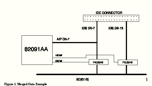
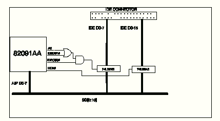
Designs that must provide a replacement primary IDE controller without a new floppy disk controller can be designed as below (figure 2). This does not provide the 3F7h data from the IDE (see note about IDE Data Address Register, below), but does not contend with another primary IDE controller when disabled.
To be sure, review your BIOS code to see if this register is ever used. We have tested this on a wide variety of applications and have found no issues. Any application that is IBM PS/2 or Model 30 compatible must not use this register since it is not available in these modes.
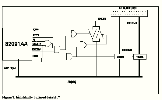
The lower byte can be buffered independently. This is only necessary if: another IDE controller is required (without the floppy controller) and that controller can not be operated in the secondary address range and the BIOS (or applications) need the data bits from the IDE 3F7h register. This requires an extra buffer to divide the data bits.
Legal Stuff © 1997 Intel Corporation
