The Problem
Two (or more) 8255As may not be directly connected together in either Mode 1 or Mode 2. Additional logic is needed.
What does it take?
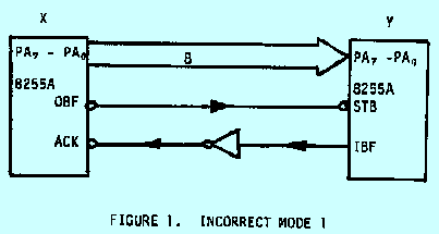
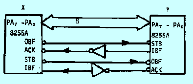
Many users attempt to form a high-speed 8-bit parallel bus using two 8255As in Mode 1 or Mode 2. At first glance, it appears that this can be done with the addition of one inverter for unidirectional transfer, and two inverters for bidirectional transfer, as shown in Figure 1 and Figure 2. In figure 1, only Port A control and data lines are shown; connections for Port B are similar.
The current 8255A AC specifications indicate that these connections will not work properly! The "handshaking" signals generated by the 8255A do not provide adequate STB pulse width and data set-up times for the input port.
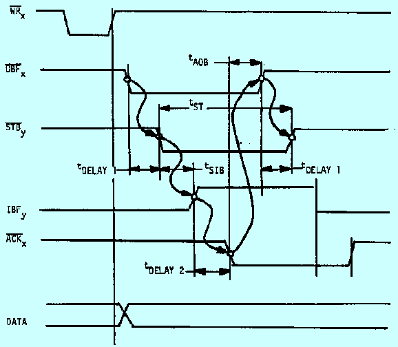
The timing diagram of Figure 3 applies to the circuits of Figure 1 and Figure 2; here the left chip (labelled X) is transmitting data to the right chip (labelled Y). The sequence of control signal transitions we are concerned with is shown by arows in Figure 3, starting with the leading edge of OBF X and ending with the trailing edge of STB Y. In the timing diagram, t DELAY1 represents the delay from OBF X to STB Y; t DELAY2 represents the delay from IBF Y to ACK X. In Figures 1 and 2, t DELAY and t DELAY2 are delays due to the inverter and the connections themselves. Data transfer fails when the minimum pulse width for STB Y (500ns) is violated. This may be analysed by following the arrows in Figure 3 from the leading edge to the trailing edge of STB Y; this is the t ST spec. The result is:
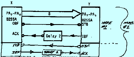
The Solution
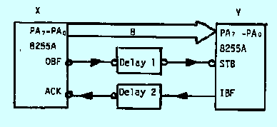
At least 500nx delaymust be inserted in the sequence of control signals. Figure 4 is the same as Figure 1, but with delay elements Delay 1 and Delay 2 added. The required delay may be generated by Delay 1, or by Delay 2, or both. It would be preferrable to use only Delay 2 since this line must contain an inverter, so inversion and delay functions may be combined (see Figure 5). The circuit of Figure 2 may be similarly modified. One delay element is needed for each port in Mode 1; two delay elements are required for each 8255A in Mode 2.
© Intel Corporation, 1992
Legal Stuff © 1997 Intel Corporation
