The 82355 is a VLSI device which integrated all the functions required to implement an EISA Master I/O device. The 82355 is designed to support a wide variety of Bus Master adapter architectures and applications.
Applications:
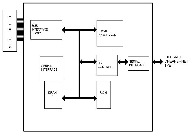
The 82355 is targeted for high performance adapter card applications. High performance adapter have a complete subsystem with the processor, memory and I/O controller on the card (Figure 1). The more common examples of high performance applications are local area network controllers, disk controllers, and graphics devices. Some additional examples of high performance applications include accelerators, multiprocessing, and FDDI.
Architecture:
The EISA system was defined with Bus Masters in mind. Man system board designs are incorporating dual port memory and concurrency which will allow simultaneous operation of multiple masters. The 82355 brings bus mastering capability and associated performance boost to adapter card designs.
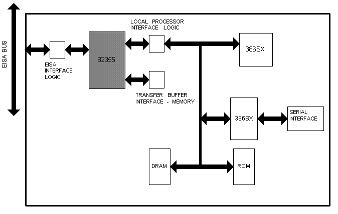
Figure 2 shows an example design of an intelligent EISA Bus Master adapter with the 82355. This particular design is for local area network application, but this architecture can be used for other applications. This design highlights the relationship of the various functional units to the 82355.
Bus Master Functions:
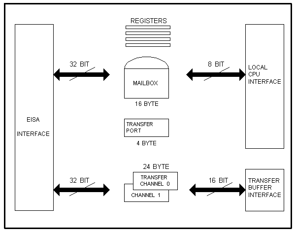
The 82355 incorporates three fully concurrent interfaces: EISA Interface, Transfer Buffer Interface, and Local Processor Interface. The EISA Interface is a synchronous interface, and it supports the EISA protocols. The EISA interface can sustain a maximum transfer rate of 33 MB/s. The Transfer Buffer Interface is a synchronous interface, and it supports high speed buffer memory designs. The buffer memory can be implemented with SRAMs or FIFOs. The maximum transfer rate on the Transfer Buffer Interface is 40MB/s. The Local Processor Interface is a generic asynchronous slave interface which allows any processor to the interfaced with the 82355 with minimal external logic.
The 82355 integrates two independent Transfer Channels. Each channel contains a 24 byte FIFO. The FIFO allows the EISA Interface and Transfer Buffer Interface to function asynchronously. The 24 bytes FIFO also provides an additional degree of latency protection. The 82355 also integrates a Transfer Port Mailbox register with Semaphore Ports, and Doorbell (interrupt) register for communication between EISA system board processor and the adapter card processor.
EISA Interface:
All of the 82355 EISA Interface signals with the exception of the data signals IDAT[31:0] and address signals IADS[31:10] are directly connected to the EISA bus. The 82355 uses seven TTL devices to interface to the EISA bus. The 82355 generates all the necessary control signals for these TTL devices.
The data lines IDAT[31:0] are connected to the EISA bus through four 74F245 data buffers (Figure 4). The 82355 generates control signals IDOE# and IDDIR for the 74F245 data buffers. The polarity of IDDIR signal forces the 74F245 A outputs (24ma) to be connected to the EISA bus, and the 74F245 B outputs (64ma) to be connected to the 82355. Although this configuration compiles with the EISA Bus Specifications for DATA current drive, it is recommended that the 74F245 B outputs (64ma) connected to the EISA bus. A 74F04 inverter in the IDDIR signal path allows for the 74F245 buffer output direction to be switch as recommenced (Figure 4).
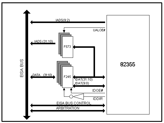
Due to pin limitations on the package, the 82355 does not have dedicated output pins for EISA address lines IADS[31:0]. The 82355 uses IDATA[31:0] pins to multiplex the IADS[31:10] signals. Three 74F573 octal latches are required to latch addresses IADS[31:10] (Figure 4). The 82335 generates UALOE# signal as the latch input to the 74573s.
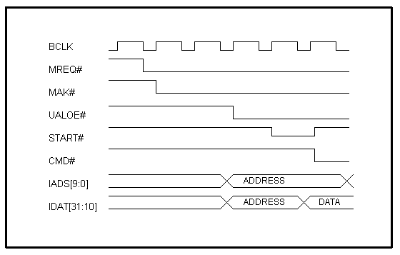
The 82355 takes advantage of the 1K page boundary defined in the EISA Bus Specifications to load the upper address IADS[31:10] in the 74F573 octal latches. Once the 82355 has been granted ownership of the EISA bus (MAK# asserted), the 82355 performs an upper address load cycle before starting data transfer (Burst or Non-Burst) on the EISA bus (Figure 5). Subsequently, during data transfer whenever a 1K page boundary is crossed, the 82355 will load the address of the new 1K page before proceeding with the data transfer.
The 82355 is a 32 bit Master device on the EISA bus and it can directly communicate with 32 bit EISA Slave devices. In the Burst mode, the 82355 can also directly communicate with 16 bit EISA Slave devices by downshifting into a 6 bit EISA Master. The 82355 communicates with 16 bit Non-Burst EISA Slaves and 8, or 16 bit ISA Slaves by allowing the EISA system board to copy the data and translate the control signals as necessary. The 82355 relinquishes the EISA bus to the EISA system board for data size translation as described in the following paragraph.
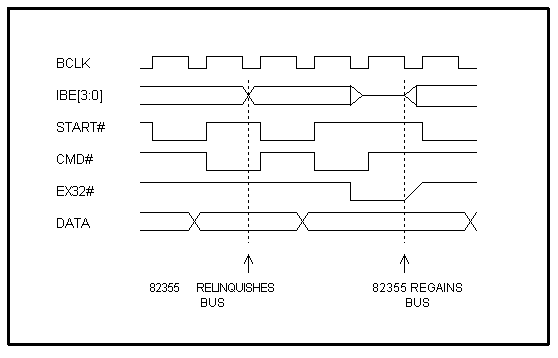
The 82355 initiates a data transfer cycle by asserting START# signal as always (Figure 6). The 82355 samples the EX32# signal and negates START# signal on the next rising edge of BCLK. A negated EX32# signal indicates to the 82355 to relinquish the control of the EISA bus to the EISA system board for data size translation. The 82355 starts to float START#, IBE#[3:0] and IDAT[31:0] (write) signals on the next following edge of BCLK. The EISA system board gains control of the EISA bus and performs the necessary data size translation cycles. The EISA system board relinquishes the EISA bus by asserting the EX32# signal. The 82355 samples the EX32# signal asserted on the rising edge of BCLK and regains control of the EISA bus on the next falling edge of BCLK.
Transfer Buffer Interface:
The 82355 Transfer Buffer Interface is a 16 bit synchronous interface. The interface is designed for high speed transfer buffer memory devices. The transfer buffer memory can be an SRAM or a FIFO. In graphics applications, the frame buffer itself can be used as the transfer buffer memory.
The 82355 Transfer Buffer Interface consists of a clock input TCLK signal, data lines TDAT[15:0], transfer protocol signals TRQ#, TACK#, and five other control signals (TDIR, TCHAN, TLD#, TDOE#, and TEOP#).
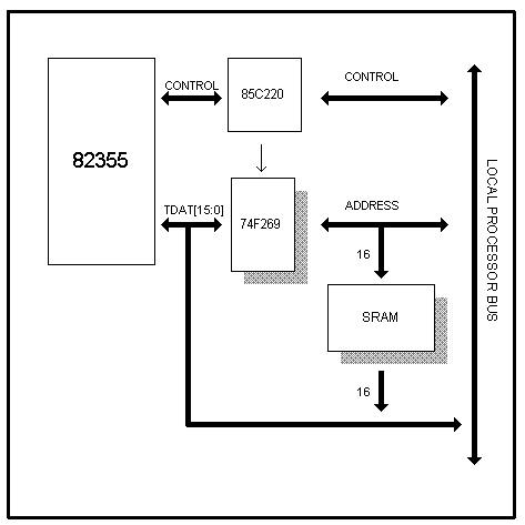
The 82355 interface to an SRAM buffer memory requires, excluding the SRAM memory, a minimum of three discrete devices (Figure 7): two 74F269 binary counters and one 85C220 programmable logic device. The 82355 uses the data lines TDAT[15:0] to drive the starting address of the transfer block in the buffer memory. The 74F269 are used to latch this starting address during the address load cycle of the 82355. During the data transfer cycles, the 74F269 binary counters provides the address of the current data transfer to the SRAMs. The 85C220 programmable logic device is used to implement state machine design to support buffer memory access from the 82355 and the processor bus. The details of the state machine design with the PAL equations will be available in an 82355 applications note to be published in April 1990. The application note will also discuss a dual port buffer memory implementation for high performance concurrent adapter card designs.
The 82355 Transfer Buffer Interface shut down after a transfer completion is initiated by the EISA interface block with the negation of the last CMD# signal in the transfer. During EISA read transfers, the 82355 Transfer Buffer Interface stops transferring data by deasserting TRQ# signal with the last word transfer. During EISA write transfers, the 82355 Transfer Buffer Interface overheads the buffer memory by a maximum of 28 bytes.
In a FIFO implementation of the buffer memory the 82355 Transfer Buffer Interface overhead will result in data lost. The overhead during EISA writes in FIFO designs requires external logic to terminate the transfer by asserting the TEOP# signal with the last word transfer. The 82355 application note to be published in April 1990 will discusss in detail different implementations for the TEOP# logic.
Local Processor Interface:
The 82355 has a generic 8 bit asynchronous slave interface for the adapter card processor. This generic interface allows any number of processors of microcontrollers to be interfaced to the 82355.
The 82355 local processor interface consists of LCS#, LWR#, LRD#, LRDY, and LINT control signals. The LRDY signal is activated only during shared register accesses. The interface timing for non-shared register accesses require an external wait state generator.
Interfacing the 82355 to a 80186 style processor is extremely simple. The programmable peripheral select and wait state generator of the 80186 allows the 8235 local processor interface control signals to be directly connected to the 80186.
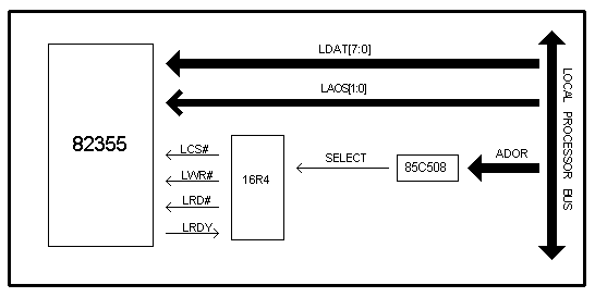
Interfacing any other processor to the 82355 requires a minimum of two programmable login devices (Figure 8). The 85C508 is used to decode the I/O space address of the 82355 registers. The 16R4 converts the adapter card processor cycles into the 82355 interface protocol. The 16R4 also contains the processor wait state generation logic. The details of the interface design for the 386SX processor with the PAL equations will be available in an 82355 application note to be published in April 1990.

Legal Stuff © 1997 Intel Corporation