For additional information about the Serial Port, refer to the 8XC196KC/KD User's Manual (order #272238) or ApBUILDER software (order #272216).
The Serial Port is a very powerful peripheral that allows the 8XC196KC/KD to communicate with other serial devices like the MCS® 51, MCS® 96, or your PC. The 8XC196KC/KD includes a Universal Asynchronous Receiver and Transmitter (UART). The UART has four different modes of operation to choose from. Three of the modes allow full duplex operation, which means that it can transmit and receive simultaneously. Another feature of the serial port is that it is receive-buffered, meaning that it can accept another byte of information before the previously received byte is read from the receive register and not lose any data.
Serial Port Basics
Serial communication comes in two basic flavors: synchronous and asynchronous.
Synchronous communication uses a clock pulse to synchronize the 8 bits of data being transferred at a time. This mode of communication has the advantage of faster speeds of transmission and more reliability compared to asynchronous communication. The drawbacks are additional wiring and more complex support circuitry than asynchronous communications.
Asynchronous communication is much simpler to implement than its clocked counterpart. This mode is the preferred choice of the computer industry. Since it is preferred we will be focusing our attention here. Because asynchronous communication lacks a synchronizing clock between the receiver and transmitter, we must have a fixed data-transfer rate. This fixed data-transfer rate is known as the baud rate. The baud rate is the number of bits transferred per second. The transmitter and receiver each generate a signal at the selected baud rate based on their respective internal system clocks. The baud rate of the receiver and transmitter can differ by about 3.0% with a maximum variance of about 5.0%.
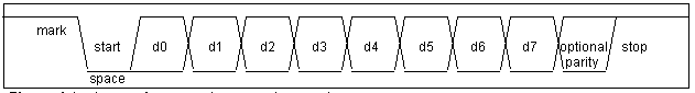
An asynchronous transmission begins with a continuous high signal (mark) on the data line when no characters are being sent (See Figure 1). The beginning of a character is indicated by a high to low transition. This transition keeps the data line low (space) for one bit time; this is known as the start bit. After the start bit has been detected, 7 or 8 data bits follow, with the least significant bit first. These bits are followed by an optional parity bit to ensure data integrity. After the parity bit has been transmitted one or more stop bits follow ensuring that the line is high for the next transmission.
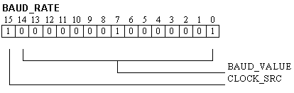
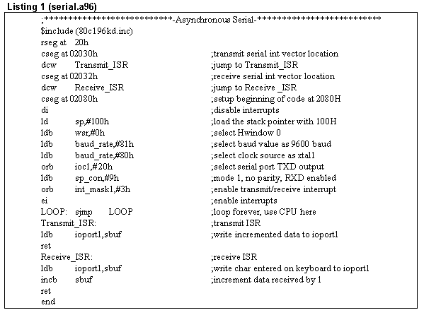
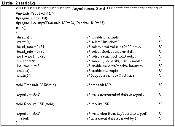
The BAUD_RATE SFR determines the baud rate and clock source for the serial port. This register must be written to one byte at a time, with the least-significant byte first. This can be seen in program listings 1 and 2 when BAUD_RATE is loaded with 81H then 80H. Bits 0 through 14 hold a BAUD_VALUE, equal to 81H, that allows communication at 9600 baud. Bit 15 (CLOCK_SRC) holds a 1, which enables XTAL1(internal source). Either XTAL1 or T2CLK can provide a clock for the baud rate generator. In this discussion we will use XTAL1 as the source for the baud rate generator. Setting bit 15 is accomplished by loading BAUD_RATE with the value 80H. Using a 20 MHz 8XC196KC/KD in Asynchronous Mode 1 the BAUD_VALUE can be calculated from the equation below letting Fosc = 20MHz (XTAL1 frequency) and Baud Rate = 9600. For more information see page C-4 of the 8XC196KC/8XC196KD User's Manual.
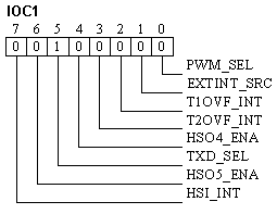
In program listings 1 and 2, IOC1 is loaded with 20H, which sets bit 5. This enables the serial TXD (Transmit) function of P2.0 (port 2 bit 0) instead of functioning as a normal output port pin. For this discussion we will be focusing on bit 5 alone, because it is the only one of concern.
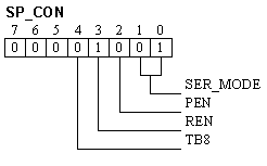
The SP_CON SFR (Serial Port Control) selects the communications mode, even parity (PEN), receive (REN), and transmit ninth data bit (TB8). In program listings 1 and 2 SP_CON is loaded with the value 9H. This enables Mode 1 (asynchronous communication) with no parity, no ninth-bit, and receive enabled. Receive enabled activates the receive (RXD) function of P2.1 (port 2 pin 1). When REN is set, a high to low transition on the RXD pin begins a reception. Bits 5 - 7 are reserved and should always be written as zeros.
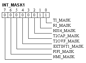
In the program listings 1 and 2, INT_MASK1 is loaded with 3H. Bits 0 and 1 are the only bits with which we need to concern ourselves. By setting TI_MASK and RI_MASK we enable the Transmit and Receive interrupts. When the Transmit interrupt is generated program flow is altered and the microcontroller vectors to memory location 2030H. When the Receive interrupt is generated the microcontroller vectors to memory location 2032H.
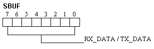
In the program listings 1 and 2, SBUF performs as a transmit (TX) and receive (RX) buffer register. SBUF can be written to and read from. SBUF(TX) when written to starts a transmission in modes 1,2, and 3. SBUF(RX) contains data received from the serial port which is double buffered so that it can begin receiving a second data byte before the first byte has been read.
Programming the Serial Port
Setting up the Serial Port can easily be accomplished by using interrupts to transmit and receive data. When an interrupt is generated, the program flow is altered. For example, the Transmit interrupt causes the microcontroller to vector to interrupt vector location 2030H. At that point a DCW command loads the location with the proper interrupt service routine location. (See program listing 1 for specifics.) In program listing 2, which accomplishes this task in C, setting up the interrupt vector location may seem more mysterious. When using C196, setting up the interrupt vector location is done by including the line #pragma interrupt(). In this case, we set our ISR (Interrupt Service Routine) name equal to the number 24. Each interrupt in C196 is associated with a number. For instance, when the Receive interrupt is desired, the name of the ISR is assigned a value of 25. See your C196 user's manual for more information and the values associated with each interrupt.
Once we have set up our interrupt vector location for Transmit and Receive we are ready to begin initialization. To begin initialization, we disable all interrupts to make sure they do not occur while we are initializing the Serial Port. One of the first SFRs we need to look at is the Stack Pointer (SP). The SP should be loaded with a value when programming in ASM196 (MCS® 96 assembly language). In program listing 1, a value of 100H is used. If you use C196 (MCS® 96 C language) some of the initialization is already done for you, so this step is not needed. When reading or writing to the SFRs it is always important to be sure that you are in the correct horizontal window or Hwindow. For example, in order to access the BAUD_RATE register Hwindow 0 must be selected. We select Hwindow 0 by loading the WSR (Window Select Register) with 0. Now that we have chosen the correct Hwindow, the BAUD_RATE register is ready to be loaded with the first byte, 81H which has been calculated previously to determine the baud rate. The next byte, 80H, is loaded into the BAUD_RATE register which selects the baud rate generator clock source as XTAL1. Then bit 5 of IOC1 is set with the ORB mnemonic and 20H. This enables IOPORT2 pin 0 to function as a serial TXD pin instead of an output port pin. Next SP_CON is loaded with 9H. This enables IOPORT2 pin 1 to function as a serial RXD pin instead of an input pin. This also selects communications mode 1 with no parity. Bits 0 and 1 of INT_MASK1 must set to enable the Transmit and Receive interrupts. This is accomplished by useing the ORB mnemonic and 3H.
Now that initialization has taken place we can enable the interrupts. While there are no transmissions or receptions, we sit in an endless loop. This endless loop simulates other instructions that the processor could be executing. The free time that the processor has can now be used to perform other activities like pulse width calculations, counting, numerical analysis or other system maintenance. At this point we are ready to set up the ISR. When using ASM196 we should issue a PUSHA upon entering the ISR and a POPA upon exiting the ISR. When using C196 this is not necessary because this has already been taken care of for us. Let's now focus on the Receive_ISR. Inside the ISR, received data is placed in the SBUF SFR. Next IOPORT1 is loaded with the value of SBUF. If this program is run on an Intel 8XC196KC/KD Evaluation board or Project Builder board, IOPORT1 drives an LED bank. This means that when data is sent to the 8XC196KC/KD it is echoed to the LED bank. SBUF is then incremented by one. When the register is incremented the new incremented value is written to SBUF which triggers the Transmit interrupt. Program flow is altered and we enter the Transmit_ISR which transmits the now incremented data to the serial port which is loaded into IOPORT1.
When program listings 1 or 2 are run on an Intel 8XC196KC/KD Evaluation board or Project Builder board serially linked to a P.C. with a communications program we can see our code in action. On the 8XC196KC/KD side load the assembled or compiled program listing 1 or 2 into memory using ECM96 or the Debug Monitor supplied with your Evaluation board or Project Builder board. Once one of the program listings has been loaded tie the EA pin of the microcontroller low by changing a jumper setting on the board you have. (See your Evaluation board or Project Builder board user's manual for the correct jumper setting to change.) Once this has been done depress the reset button. By tying the EA pin low the microcontroller accesses external memory upon reset instead of internal OTP EPROM. Once the reset button has been depressed the program is running. On the P.C. side make sure that your communications program is initialized to utilize the correct COM port setting for your serial cable. Also make sure that your communications program is set up at 9600 baud, no parity and 8 data bits. Once all this has been done we are ready to test the program. When a key is pressed on the P.C. keyboard it is serially transmitted to the microcontroller. Upon reception the data is echoed to the LED bank and the data is incremented by one and echoed again to the LED bank and transmitted to the P.C.. Since the data has been incremented it will now show up on the P.C. one ASCII character higher. This means that when an "A" is pressed on the P.C. keyboard the binary representation of "A" (01000001) is briefly displayed on the microcontroller LED bank. Then the binary representation of "B" (01000010) will show up on the LED bank and a "B" will appear on the P.C. communications program screen. This demonstrates the functionality of the 8XC196KC/KD serial port in the asynchronous communications mode.
PROGRAM LISTINGS: Program listings 1-2 can be found in the following files: BTBEVAL.EXE for evaluation boards and, BTBDEVEL.EXE for Project Builder boards on the Intel Bulletin Board Service in the MCS®(R) 96 Family / General section. The program filename is serial.a96 and serial.c.
Legal Stuff © 1997 Intel Corporation
