Bootstrap and Programming modes of 87C196KX Devices
The Bootstrap and Programming modes are new features of all 87C196KX microcontrollers including the KR, JR, KQ and JQ, and all future derivatives of the KX core. The simple hardware set up of these modes makes them useful tools for in-module testing and programming and in-line diagnostics.
The bootstrap mode allows the user to
Once in the test mode, the device will begin to execute a RISM (Reduced Instruction Set Monitor) program. The user communicates with the device by sending special RISM commands across the serial port from any smart terminal. The commands direct the RISM to read and write memory locations or to run programs which h read and write to memory.
Since the RISM begins at location 2000h in EPROM, the user EPROM is automatically remapped to location A000h. Parameters for RISM operation such as baud rate and programming pulse width are contained in reserved locations in the test ROM. The parameters are initially set at their default values but may be changed to conform to almost any operating conditions the user requires.
Special software called IBSP196 simplifies communication with the device through a PC terminal.
Request IBSP196 free of charge through you local Intel sales office or factory.
Hardware Requirements
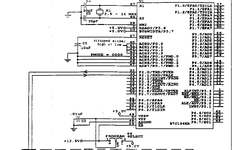
To put the device into the test mode, the following voltages must be applied on reset. With the hardware configuration shown in Figure 1, the device will reset on power down. Since this is a CHMOS device, all input-only pins (40-43) must be held either all high or all low.
| 1.25 V to pin | 29(EA) | Selects test mode |
| 0V to pins | 44-47 (PMODE, P0.4-P0.7) | Chooses Bootstrap and Programming modes |
Also apply
| 5 V to pins | 2 (Ready), 10 (Buswidth), 31(VCC), 49(Vref) |
| 0V to pins | 28 (NMI), 5, 30, 68 (VSS) , 48 (Angnd) |
Programming Mode: VPP (pin 6) = 12.5V. Required for programming internal EPROM locations
(0A000h-0DFFFh).
Bootstrap Mode: VPP (pin 6) = 5V. Allows programming to code RAM (400h-4FFh), but does not allow programming to internal EPROM.
Both modes allow the user program to execute from either EPROM or coed RAM. The device must be in the programming mode if the program mode if the program performs any writes to EPROM locations since writing follows the same algorithm as programming (see section RISM Commands). Breakpoint support is available while operation out of code RAM or external RAM, but not during operation out of internal EPROM.
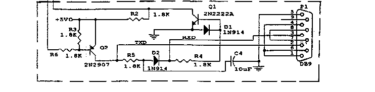
Transmission and reception over the serial port is through TXD (pin32) and RXD (pin33). These pins should be connected to any smart terminal able to communicate with the RISM. Any host such as a PC which requires an RS-232 interface must be connected through an RS-232C driver/receiver such as the one within the dashed line in Figure 1.
Xtal1 (pin67) AND Xtal2 (pin66) may be connected to a crystal or ceramic resonator between 3.5 and 16 MHz. This clock frequency MUST match the value in the Serial Port Baud Rate Register (location 2214h). See section Changing Defaults.
The RISM is located in memory from 2000h -23FFh, with program execution beginning at 2080 as usual. The RISM is only operable while the user is in the test mode, remapping the internal user EPROM to locations 0A000h-0FFFFh. A memory map of normal operation. Since this map applies to all KX devices, see the not below to determine which addresses are valid for each memory size.
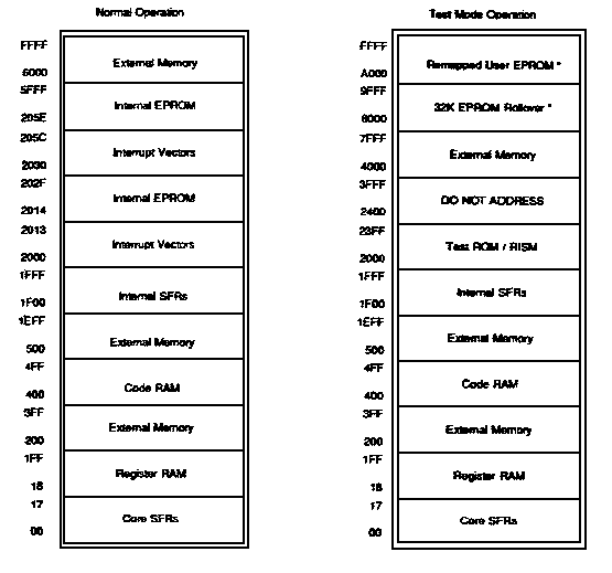
Any memory in the address range A000h-FFFFh which is not remapped as user EPROM is undefined and SHOULD NOT BE USED.
Changing Defaults
The test ROM assumes 16MHz operating frequency, serial port baud rate of 9600 baud, 8 bit no parity, and one stop bit. Special locations in EPROM may be altered to change these defaults.
| 2213 | Serial Port Control (byte) |
| 2214 | Serial Port Baud Rate (word) |
| 2216 | Programming Pulse Width (word) |
| 2218 | Chip Configuration Byte 0 (byte) |
| 221A | Chip Configuration Byte 1 (byte) |
Before any programming, it is first important to change the Programming Pulse Width.
Like these other special EPROM locations it is erased to 0FFFFh on exposure to UV light. This default value creates a pulse width of 8.74 seconds which must elapse each time a work is written. To shorten the write time to an appropriate amount, determine the PPW from the table or equation below and program location 2216h (See Example 1). The MSB of the PPW must always be set to one.
| Frequency | PPW | Cumulative PPW |
| 6 MHz | 8003h | 2.13 ms |
| 8 | 8004h | 2.0 |
| 10 | 8005h | 1.92 |
| 12 | 8007h | 2.13 |
| 16 | 8009h | 2.0 |
The cumulative PPW is 25 times as great since the internal program loops through the program cycle 25 times. (This is now 5 times)

Where Tosc depends on the operating frequency.
Remember, these are minimum values. If the PPW is too short, write operations may not be completed. Larger values will cause the user to wait longer any time a memory location is altered.
Coordinating Baud Rate with Operating Frequency:
The Serial Port Baud Rate Register (2214h) must correspond to the frequency on Xtal or the device will lose communication through the serial port. The default value 0FFFFh assumes 9600 baud and Xtal= 16MHz. Changing the value at 2214h sets the special function register SP_Baud at location 1FBCh, although no change is needed unless a different operation frequency or baud rate is desired. To determine the value for the baud rate register, use the following relation between baud rate and operating frequency:

For example, changing Xtal to 12MHz at 9600 baud would require a value of 804Dh programmed into location 2214h. The MSB of the Serial Port Baud Rate Register must always be set to one to select Xtal as the input for operating frequency.
Remember that once the value in any EPROM location is changed, any bit which has been cleared to zero cannot be reset to one without erasing the entire EPROM.
User PC, WSR, PSW:
The default of the Program Counter is 2080h since this is the beginning of the test ROM. The Window Select Register is set to 1000h to enable only the serial port interrupt and the Program Status Word is set to 0200h to set the global interrupt flag. These values may be changed by changing the following locations:
RISM commands
The RISM is in a constant "pause" condition, waiting for instructions across the serial port in the form of RISM commands. The commands are each one byte in length and have values between 00h and 1Fh. Each time a command appears on the serial port, it is read into the internal RAM location CHAR at 56h. Any characters read from the serial port with values greater than 1Fh are assumed to be data and are read into a 32 bit FILO (First In Last Out) memory location DATA at 58h. Each time new data comes in, the DATA register is shifted left long by eight bits.
Any data values less than 1Fh must be preceded by a DLE (Data Latch Enable) command to alter the RISM that the next character should be stored in the DATA register. DLE must be sent prior to each character of data which is less than 1Fh, including data values between 00h and 1Fh which do not correspond to a RISM command.
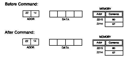
To access a particular address, the address must first be sent across the serial port one byte at a time as data. Then the address must be transferred to the address register ADDR at 5Ch using a data-to-address command. The address is always assumed to be 16 bits. Examples of this procedure can be found with the write and read command descriptions, as well as in the section RISM Command Examples.
| RISM Commands | Value |
| DLE Xmit Read_byte Read_word Write_byte Write_word Data_to_addr Indirect Go Halt Report | 00 02 04 05 07 08 0A 0B 12 13 14 |
DLE (00h):
Sets the DLE flag bit 0 of MODE (57h: byte) to tell the RISM that the next character on the serial port will be data and should be loaded into the DATA register at 58h. The flag is cleared again as soon as the character is read.
XMIT (02h):
Transmits the data in the low byte of the DATA register to the serial port through location CHAR and shifts the whole DATA register right long by eight bits. Also increments the address in the address register by one.
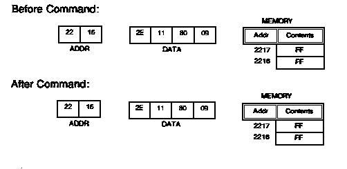
READ_BYTE (04h):
Puts the contents of the address in the ADDR register into the low byte of the DATA register.
READ_WORD (05h):
Same as Read_byte except the word at the address in the ADDR register is loaded into the low word of the DATA register.
After Command:

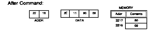
WRITE_BYTE (07h):
Puts the low byte of the DATA register into the address contained in the ADDR register. Also increments the ADDR register by one.
Same as Write_byte except that the low word of the DATA register is placed into the address contained in the ADDR register, increments the ADDR register by two.
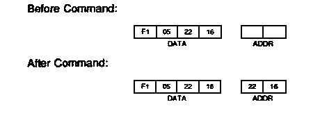
Data_to ADDR (0Ah):
Puts the low word of the DAT register into the ADDR register. The address is always a word.
Puts the word in the address contained in the ADDR register into the ADDR register.
Pushes the user PC, PSW, and WSR onto the stack and starts the user program from the location contained in the user PC. The RISM PC, PSW, and WSR will be buried in the stack so it is important to allow enough room on the stack for all six words.
The user may interrogate memory locations while the program is running. Sending RISM commands across the serial port interrupts the user program while the command is processed and then returns execution back to the user program.
The user program should not directly alter memory locations 56h through 5Ch. These locations are used by the RISM if the user reads or writes to any memory during program execution.
Halt (13h):
Stops execution of the user program and puts the RISM back in the pause mode. The user WSR, PSW, and PC are removed from the stack. The PC will be set to the location of the RISM pause routine and will be pushed onto the stack. The default values of the PSW and WSR will also be pushed onto the stack.
Report (14h):
Loads a value into the DATA register corresponding to the status of the user program. The Data register will receive 00 if the user program is halted, 01 if the user program is running, or 02 if the user program is trapped.
RISM Command Examples
These examples, at the RISM command level, correspond to the examples found in the IBSP196 section.
Example 1: Programming the appropriate value of the Programming Pulse Width.
This should be done before any other programming or writing to memory locations. This example will load the PPW register at location 2216h with 8009h, the minimum value for 16MHz operation. To determine the correct PPW for other frequencies, see section Changing Defaults.
Since an EPROM location is being altered, the device must be in the Programming Mode (VPP=12.5V). This location is currently at its erased value of 0FFFFh, so PPW - 8.74 seconds.
This program step will take 8.74 seconds to complete. Ignore any transmissions across the serial port during this time. Future program/write operations will take only 2.0 ms.
Remember that RISM commands must be sent across the serial port one byte at a time, with each byte of data that is less than 1Fh being preceded by the DLE. The address being modified must first be loaded into the DDATA register and then transferred to the ADDR register.
| Send | Comments |
| 22 | High byte of address to DATA register (no DLE needed since value is greater than 1Fh) |
| 00 | DLE tells RISM that next byte is data below 1Fh |
| 16 | Low byte of address to DATA register |
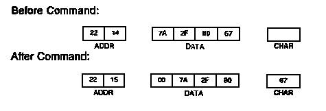
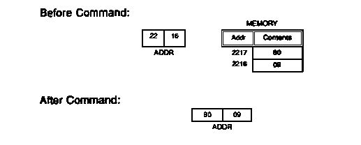
At this point the data register looks like :
| 22 | 16 |
The 22 was automatically shifted left when the 16 was received.
| 0A | Moves 2216h from Data to ADDR register |
| 80 | High byte of data to DATA register (no DLE needed) |
| 00 | DLE for next data <1F |
| 09 | Low byte of data to DATA register |
Now the DATA and ADDR registers look like:
| 22 | 16 | 80 | 09 | 22 | 16 |
08 Writes the data in the low word of the DATA register into the location contained in the ADDR register.
Any write operation may be done in this manner.
Example 2: Reading EPROM contents.
This example will read the contents of EPROM address 0A080h. Since the internal EPROM is remapped from 2000h to 0A000h, this location will actually be location 2080h of the program in the EPROM. No memory locations will be changed in this example so it is not important that the device is in the Programming Mode. VPP at either 12.5V or 5V will work.
| Send | Comments |
| A0 | High byte of address to DATA register |
| 00 | DLE for next data <1Fh |
| 80 | Low byte of address to DATA register |
| A0 | 80 |
| 0A | Transfers address from DATA to ADDR register |
| 05 | Reads word at 0A080h and places it in low word of DATA register. This number will be the assembled hex value of the code (at location 2080h of programmed EPROM). |
| 02 | Transmits the low byte of the DATA register across the serial port, increments the value in the ADDR register by one, and shifts the DATA register right long by eight bits. |
| 02 | This command must be sent twice to transmit the whole word in the DATA register. The address will be incremented again to 0A082h. Sending consecutive read instructions followed by a transmit for each byte will allow a sequential string of memory to be read. |
Any address is read in this manner, including those in register RAM, code RAM, and Special Function Register.
Example 3: Loading a simple program to code RAM and executing.
Again the example does not write to any EPROM locations, so 12.5V is not required at VPP.
The program to be loaded is:
| 400 | A122180 | LD 80h, #1122h | Puts value 112h in register RAM location 80h |
| 404 | 27FE | Sjmp 0404h | Jumps to itself to keep program running indefinitely. |
The next file must be loaded byte by byte using the RISM commands.
| Send | Comments |
| 00 | DLE for next byte of date less than 1Fh |
| 04 | High byte of address 0400h |
| 00 | DLE for next data <1Fh |
| 00 | Low byte of address |
| 0A | Transfer address from DATA to ADDR register |
| A1 | High byte of hex file intended for location 401h (no DLE needed) |
| 22 | Low byte of hex file intended for location 400h |
| 08 | Write the work 0A122h to location in ADDR register 400h |
Repeat this procedure for 1180 at 402h and 27FE at 404h, remembering to preceded any data less that 1Fh by the DLE command.
The PC at location 4Eh must be set at 400h to tell the RISM where to start user program operation. The WSR and PSW are automatically set to their default values of 1000h and 200h, respectively. The WSR and PSW could be changed if necessary in the same manner as the PC.
| Send | Comments |
| 00 | DLE for next byte of date less than 1Fh |
| 00 | High byte of address 005Eh |
| 5E | Low byte of PC address |
| 0A | Transfer address from DATA to ADDR register |
| 00 | DLE for next data < 1Fh |
| 40 | High byte of program address 0400h |
| 00 | DLE for next data < 1Fh |
| 00 | Low bye of program address |
| 12 | Go command begins program execution at user PC address 400h. If the user had changed the WSR and PSW, theses values would be placed into the WSR and PSW registers. |
Memory locations can now be interrogated using RISM commands. Reading location 80h using the method shown in Example 2 will return the value 1122h.
A report command (14h) will place 01 into the DATA register to tell the user a program is running.
Reading memory location 5Eh will return 404H since the user PC is at this location while the user program jumps to itself.
A Halt command (13h) stops execution of the user program. The PC will return to the location of the RISM pause and a Report command would place 00 into the DATA register.
Writing to EPROM using this example: If instead, the simple program attempts to write EPROM location 0A500 with the value 1122h, 12.5V must be applied to VPP. However, changing this address would alter any code programmed at 2500h (since it has been remapped to 0A500h). Any bits at this location which were already zero could not be reset to one.
If instead, this simple program is to be loaded into EPROM locations 0A000h through 0A004h, the same warnings apply. VPP must be set to 12.5V while the program is loaded and the EPROM program form 2000h to 2004h will be altered, although possibly not with the values expected if the user attempts to reset zero bits. (code RAM may always be altered to any value).
IBSP196
This software is available free of charge to facilitate communication with the 87C196KX from a personal computer. Simple IBSP196 commands sends strings of RISM commands across the serial port to read and write memory locations. A list of these commands and their proper format may be seen by typing HELP at any time while using the software.
The same VPP requirements apply for writing/programming EPROM contents as when communicating at the RISM command level. VPP must be at 5V on start up for the RISM to recognize IBSP programming. Once the IBSP916 screen appears, VPP may be changed to 12.5V for ERPOM programming. Xtal must also equal the default value of 16MHz at start up. Once the Baud Rate Register (2214h) is changed to accommodate another operating frequency, IBSP196 will lose communication with the serial port until the new Xtal is installed.
The following examples correspond to the examples in the RISM Commands section. It is suggested that the user first review that section to fully understand the operation of the RISM and ISBP196.
Example 1: Programming the appropriate value for the Programming Pulse Width.
As in the RISM Command Examples section, this example programs 8009h (for 16MHz operation) into the PPW Register at location 2216h. Remember that writing to an EPROM locations is the same as programming, so VPP must be 12.5V to put the 87C196KX into the Programming Mode.
This program step should be done before writing to other locations and will take 8.74 seconds to complete. IBSP196 will send "lost communication" messages over the serial port during this time.
Type: Word 2216=8009
The command WORD tells the RISM to access the word at location 2216h (the default value of all numbers is hex). The =sign tells the RISM to assign the value 8009h to this location. The string of RISM commands corresponding to a write operation (shown in RISM Commands Example 1) is sent across the serial port by IBSP196.
Writing to code RAM is done the same way except that VPP need not be at 12.5V. A series of memory locations could be written to at once by typing, for example.
WORD 400 to 4FE-0FFFF
This would effectively erase all locations from 400h through 4FEh with all ones. Notice the zero before FFFFh. A leading zero is required by IBSP196 for any data or address beginning with an alpha character.
Example 2: Reading EPROM contents.
This example will read the contents of EPROM address 0A08h. Since the internal EPROM is remapped from 200h-5FFFh to 0A000h-0DFFFh, this location will actually be location 2080h of the program in the EPROM. No memory locations will be changed in this example so it is not important that the device is in the Programming Mode. VPP at either 12.5V or 5V will work.
Type: WORD 0A080h
A carriage return tells the RISM that location 0A080h only needs to be read. IBSP196 will then return the following:
WORD 0A080=FFFF->
Where FFFF represents the contents of 0A080h. The cursor will be directly to the right of the arrow waiting for a value. Entering a new number at this point is another way to program an address. If no changes are to be made, a carriage return is required before entering any other IBSP196 commands.
It is also possible to read a sequence of memory locations by typing, for example,
WORD 0a080 TO 0A08E
Byte locations may be written (and read) by using the BYTE command.
Example 3: Loading a simple program to code RAM and executing.
Again this example does not write to any EPROM locations, so 12.5V is not required at VPP.
The program to be loaded is:
| 400 | A1221180 | Ld 80h, #1122h | Puts value 1122h in register RAM location 80h |
| 404 | 27FE | Sjmp 0404h | Jumps to itself to keep program running indefinitely |
| Type: | WORD: 400=0A122 | Program hex file into memory |
| WORD 402=1080 | ||
| WORD 404=27FE | ||
| WORD 5E=400 | Set user PC at location 5Eh to 400h Begin executing program at 400h |
The hex file may be disassembled to check the program.
Type: DASM 400 TO 404
Some programs may also be entered using the line-by-line assembler. Typing ASM 400 will prompt the user to enter each line of code beginning at 400h. Unfortunately this assembler does not support some of the MCS-96 instructions such as SJMP. After all assembler lines have been entered, type END.
Writing to EPROM using this example: This simple program could be loaded directly into EPROM beginning at location 0A000h form a PC file by typing PROGRAM <pathname> while VPP is at 12.5V. The file is assembled at 200h, but the PROGRAM command will automatically offset each address by 8000h. The program appears to be aligned to A000h, occupying an appropriate amount of space depending on the size of the EPROM in a particular device, but is still resides at 200h in the normal operation mode.
Some restrictions apply when writing to EPROM. See the end of Example 3 in the RISM Commands section for an explanation of the warnings, as well as suggestions for having the simple program alter EPROM locations.

Legal Stuff © 1997 Intel Corporation