For additional information about the High Speed Output, refer to the 8XC196KC/KD User's Manual (order #272238) or ApBUILDER software (order #272216).
The High Speed Output (HSO) is a very powerful peripheral that allows the 8XC196KC/KD to trigger programmable events at specified times with minimal CPU overhead. These programmable events include starting A/D conversions, generating software timer delays, toggling HSO output pins or resetting Timer2. All these events can be triggered from either Timer1 or Timer2. These features are very useful in applications like motor control, anti-lock braking, D/A conversion and wave form generation.
HSO Functionality
The HSO module will trigger an event at a specified time. This peripheral can be configured to toggle 1 of 6 output pins high or low, generate an interrupt from 1 of 4 software timers, reset Timer 2 or start an A/D conversion. Both the pending events and times are stored in a Content-Addressable Memory (CAM) file. The CAM file is capable of storing up to 8 events and times. Once these events and times are loaded into the CAM, the HSO compares all 8 CAM entries with the timer before triggering an event. One state time per CAM entry is required for comparing values in the CAM. This translates to eight state times to perform a full CAM search. Up to 15 different events may be triggered by the HSO. When Timer2 is used as a reference timer, it is important to operate the timer in the normal mode (not the fast increment mode). It is also very important to wait up to 8 state times before loading a new event into the CAM. This allows time to move the event from the Holding Register into the CAM ensuring that a previously written entry will not be overwritten.
1 state time = [2/crystal frequency (Mhz)]
Registers Involved with the HSO
There are several Special Function Registers (SFRs) that are essential to programming the High Speed Output. In the text that follows some of the key HSO SFRs will be described in detail. Let's begin by discussing the HSO_COMMAND register.
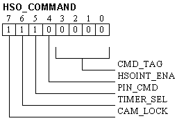
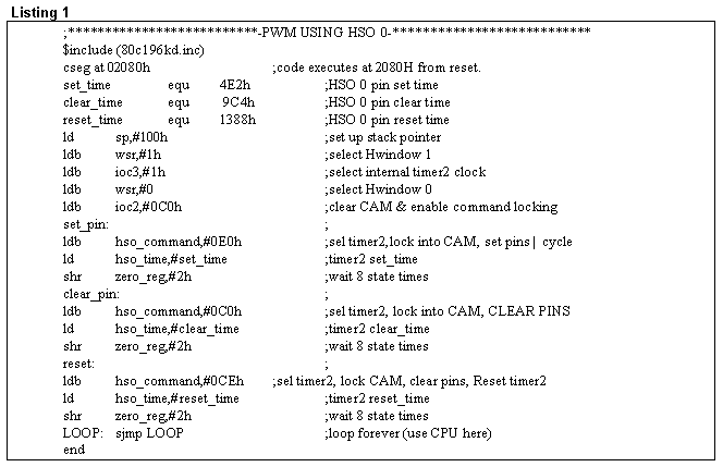
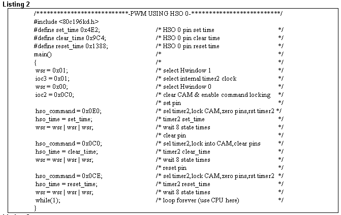
The HSO_COMMAND SFR determines what events will occur at the specified time. At one point in program listing 1 we load HSO_COMMAND with E0H. This locks the event into the CAM, selects Timer2, sets the pin, and selects HSO.0. Bits 0-3 control what events will take place. The value of these bits can range from 0 to 15. In program listings 1 and 2 CMD_TAG is loaded with 0, while in listings 2 and 3 CMD_TAG is loaded with 8. (See page 8-19 of the 8XC196KC/KD User's Manual for more information about the different events that can be programmed into the HSO.) When Bit 4 is enabled an interrupt will be generated. This is useful for running a routine at a specified time for each timer cycle. When Bit 5 holds a 1 the HSO pin is set, otherwise the HSO pin is cleared. Bit 6, when set, selects Timer2 and when clear selects Timer1. Bit 7 determines whether an event is locked into the CAM. If a command is not locked then it will be cleared from the CAM after execution. A CAM entry that is locked can be canceled by issuing a complementary command with the same time tag or by clearing the entire CAM by setting bit 7 of the IOC2 register.
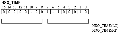
HSO_TIME is a 16 bit register that specifies the time that an HSO event will occur. At one point in program listing 1, HSO_TIME is loaded with 4E2H. This is the time that an event will be triggered. When events are written to the CAM, make sure that the HSO_COMMAND SFR is written to before the HSO_TIME SFR. The values that HSO_TIME can be loaded with range from 0 to FFFFH.
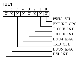
In program listings 1-4, IOC1 is omitted because we will not be using HSO lines 4 or 5. If we did want to use these HSO lines we would need to set bits 4 and 6 to enable them as outputs. In this discussion these bits are the only ones with which we need to concern ourselves.
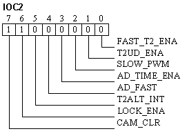
In program listings 1-4, IOC2 is loaded with C0H. This enables command locking of the CAM and clears all entries that may already be there. Bit 0 is responsible for enabling the fast increment mode when Timer2 is used. For our purposes we must disable the fast increment mode by placing a 0 in that bit. Bit 1 allows us to count in an upward or downward direction. In the program listings an upward direction was chosen. Bit 6 enables command locking capabilities in the CAM. Lastly bit 7 determines whether all the entries in the CAM are cleared.
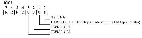
IOC3 SFR is used in program listings 1 and 2. Bit 0 determines whether Timer 2 is clocked internally or externally. By placing a 1 in this bit we select an internal source and by placing a 0 in this bit we choose an external source. In listings 1 and 2 we will use an internal source to clock Timer2. Bits 1-7 do not concern us in this discussion and will not be described here.
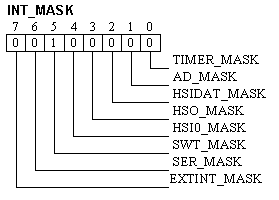
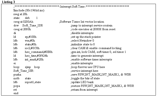
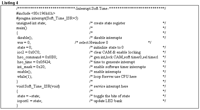
In the program listings 3 and 4, INT_MASK is loaded with 20H. Bit 5 is the only bit with which we need to concern ourselves. By loading bit 5 with 1 the Software Timer interrupt is enabled. When this interrupt INT05, occurs program flow is altered and the microcontroller will vector to memory location 200AH.
Overview of programming the HSO
In the discussion that follows we will be discussing two important applications of the HSO. Both of these applications rely on the timers. One of the applications generates a Pulse Width Modulation (PWM) with the HSO. The other application generates an interrupt based on the Software Timer. The HSO is very useful because it does not seriously burden the processor with unnecessary overhead. Program listings 1 and 2 generate a PWM based on Timer2, while listings 3 and 4 generate interrupts based on Timer1. Both applications are designed to use Timer1 and Timer2 independently to show the nuances of programming each timer.
An important aspect of programming the HSO is determining how many timer ticks (the unit of time required to increment the timer by 1) are necessary to create the appropriate delay. To calculate the proper delay we need to do a few calculations.
One state time = [2/crystal frequency (MHz)].
One timer tick = 8 state times {Assuming we don't use fast increment mode}
= 8*100ns
= 800ns
Desired delay = 1ms {Assume value of 1ms for simplicity}
= 1ms/800ns {Calculate delay in timer ticks}
= 1,250 timer ticks
= 4E2 hexadecimal
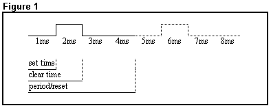
From our previous calculations we found that a 1ms delay was equivalent to 4E2H. This is the value of the user-defined register set_time in program listings 1 and 2. Clear time (see figure 1) occurs at exactly 2ms. This is twice the value of the user-defined register set_time or 9C4H. This is the value of clear_time in listings 1 and 2. Lastly the period or reset value occurs at 4ms. This is four times the value of set_time or 1388H. In program listings 1 and 2 this is the value of reset_time.
We are now ready to begin programming the previously calculated values into the HSO. One of the first SFRs we should take a look at is the Stack Pointer (SP). The SP should be loaded with a value when programming in ASM196 (assembly code). In program listing 1, a value of 100H is used. If you use C196 (C-code) some of the initialization is already done for you, so this step is not needed. When reading or writing to the SFRs it is always important to be sure that you are in the correct horizontal window or Hwindow. For example, in order to access IOC3, Hwindow 1 is selected. We select this Hwindow by loading the WSR (Window Select Register) with 1. Now that we can access IOC3, bit 1 is set to select Timer2 to be clocked internally. This is an important consideration when using Timer2 that is not required when programming Timer 1. From here we need to switch from Hwindow 1 to Hwindow 0. This task is accomplished by loading WSR with 0. After loading WSR with 0 we need to clear the CAM and lock new entrees. This is accomplished by assigning a value of C0H to IOC2. Since we have finished initializing we are ready to set the HSO pin high. In listings 1 and 2 HSO.0 is used. To select Timer2, lock the CAM and set the HSO pin high, load HSO_COMMAND with E0H. To associate a time with the action of setting the pin, load HSO_TIME with the user defined register set_time. Eight state times must elapse before loading a new command. This delay is accomplished by shifting right the contents of the ZERO_REG SFR twice. Now we are ready to clear the HSO pin by loading HSO_COMMAND with C0H. To associate a time with clearing the pin, load HSO_TIME with the contents of the user defined register clear_time. Again we must wait 8 state before loading in a new event. This is done by shifting ZERO_REG again. After shifting ZERO_REG we need to set up the Timer2 reset time. We want to clear the pin, lock the CAM, select Timer2 and reset Timer2. This is done by loading HSO_COMMAND with CEH. All that is left to do is load HSO_TIME with the user defined register reset_time. Now that the HSO has been set up we sit in an endless loop simulating other tasks that the CPU could be doing. To test the specifications that we have set up we can connect an oscilloscope between the HSO output pins and ground to verify that the wave form meets our expectations.
Now that we are capable of generating PWMs we can accomplish a great deal of real world tasks. If we are creative enough we can generate an interrupt every time the HSO is triggered. This will allow us to change the duty cycle, frequency and other characteristics of a wave form on the fly. This could be useful in applications like stepper motor control and anti-lock braking systems. If speed and rapid transition are an issue then a look up table of values can be constructed to decrease the need for CPU intervention. All this can aid us in creating any type of wave form with the help of a filter. If we desire a ramp function then a simple RC circuit can be placed on the HSO output. This would suffice as a rudimentary filter. If we wanted to get more sophisticated we could generate a sine wave using a 2 pole filter. If we were inclined we could even generate the wave forms required to drive a 3 phase induction motor by using 3 HSO channels in combination with filters.
Programming the HSO to Generate Software Timer Interrupts
In this section we would like to generate an interrupt at a specified time. When an interrupt is generated program flow is altered. For example, the HSO Software Timer interrupt causes the microcontroller to vector to interrupt vector location 200AH. At that point a DCW command loads the location with the proper interrupt service routine location. (See program listing 3 for specifics.) In program listing 4, which accomplishes this task in C, setting up the interrupt vector location may seem more mysterious. When using C196, setting up the interrupt vector location is done by including the line #pragma interrupt(). In this case, we set our ISR (Interrupt Service Routine) name equal to the number 5. Each interrupt in C196 is associated with a number. For instance, if an HSI Data Available interrupt is desired the name of the ISR is assigned a value of 2. See your C196 user's manual for more information and the values associated with each interrupt. The Software Timer interrupt is useful for running a piece of code at a set time. Let's assume that we would like to generate an interrupt once every 50 ms. From the previous section we concluded that 1 timer tick equals 800ns. To calculate the number of timer ticks needed, all we need to do is divide the 50 ms delay by 800ns. This yields 62,500 timer ticks. This number is equal to F424H. From program listings 3 and 4 it can be seen that this is the value loaded into the HSO_TIME register.
Let's take a look at programming the Software Timers. The first task to accomplish is to disable interrupts from occurring. This will ensure that no interrupts occur during initialization. One of the first SFRs that we should look at is the Stack Pointer (SP). The SP should be loaded with a value when programming in ASM196. In program listings 1 and 3 a value of 100H is used. If C196 is used, some of the initialization is already done for you, so this step is not needed. When reading or writing to the SFRs it is always important to be sure that you are in the correct Hwindow. In listings 3 and 4 we select Hwindow 0 by loading the WSR with 0. The next step initializes the user-defined register, state, with a value of 0. IOC2 is loaded with the value C0H, to enable command locking and clear the CAM. To generate an interrupt, lock a command into the CAM, choose software timer 0, and select Timer1, load HSO_COMMAND with B8H. Next, HSO_TIME is loaded with the value F424H, which was previously calculated. To generate an interrupt we need to select the Software Timer interrupt INT05 by setting bit 5 of the INT_MASK SFR. This allows the Software Timer interrupt to occur once interrupts are enabled. While no matching timer values are encountered we sit in an endless loop. This frees up resources to do other things like pulse width calculations, numerical analysis, or other system maintenance. We are ready to set up the ISR. In assembly a PUSHA should be issued upon entering the ISR and a POPA upon exiting. In C this is not necessary because it is already taken care of. Inside the ISR we bit-wise NOT the value in the user-defined register state. The next instruction loads IOPORT1 with the value of state. If this program is run on an Intel 8XC196KC/KD Evaluation board or Project Builder board, IOPORT1 drives an LED bank. This program toggles the output of IOPORT1 or the LED bank on and off at 50 ms intervals, assuming we use a 20MHz crystal. This will appear to the naked eye as a flickering display, but if we place the output on an oscilloscope we see a 50% duty cycle square wave transitioning every 50ms.
PROGRAM LISTINGS: Program listings 1-4 can be found in the files, BTBEVAL.EXE for evaluation boards and, BTBDEVEL.EXE for Project Builder boards on the Intel Bulletin Board Service in the MCS(R) 96 Family / General section.
Legal Stuff © 1997 Intel Corporation
