For additional information about the Analog to Digital Converter, refer to the 8XC196KC/KD User's Manual (order #272238) or ApBUILDER software (order #272216).
The Analog to Digital Converter is a very powerful peripheral that quantizes a continuous signal into a series of discrete values. The A/D converter can be interfaced to transducers that convert different forms of energy into an electrical signal. For example, we can measure things like temperature, magnetic field intensity, pressure, sound, strain, or even light intensity by interfacing the appropriate sensor to the 8XC196KC/KD's analog input channel. This peripheral allows us to sample real world inputs and manipulate the data or perform control based on that input.
Theory Behind Conversion
The A/D converter converts input voltages, in the range of 0 to 5 volts DC, into a discrete 8 or 10 bit digital representation. To begin the conversion, one state time is allowed to elapse so that the successive approximation register can be reset and the designated multiplexed channel can be selected. The sample capacitor is then connected for the duration of the sample time. Once the sample time elapses, the sample window closes and the capacitor is disconnected from the multiplexer and conversion begins. The conversion is accomplished by using a successive approximation algorithm. This technique compares the analog input to a sequence of reference voltages by using a binary search. The search continues until 8 or 10 tests have occurred. The number of tests depend on the number of bits of accuracy you have chosen. Once these tests are finished a valid conversion result will reside in the successive approximation register.
Registers Involved with the A/D Converter
There are several Special Function Registers(SFR) that play a vital role in programming the A/D Converter. In the text that follows some of the key A/D SFRs will be described in detail. Let us begin by discussing the AD_TIME register.
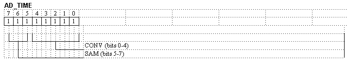
In program listings 1-4 AD_TIME is omitted because we will be using the 80C196KB-compatible mode for simplicity. Bits 0-4 are responsible for the time to convert the analog voltage, on the sample capacitor, to a digital value. The (CONV) time must range from 2 to 31 inclusively. Bits 5-7 control the sample time(ms), which is the length of time that the analog input channel is connected to the sample capacitor. The (SAM) time(ms) must range from 1 to 7 inclusively. NOTE: the values in the AD_TIME register will not be recognized unless bit 3 of the IOC2 SFR is set. For more information on calculating the (SAM) and (CONV) times, please see pages C-11 and C-12 of the 8XC196KC/KD Users Manual.
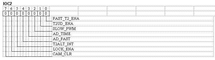
In the program listings a value of 0 is loaded into IOC2. Bits 3 and 4 are the only ones that we need to concern ourselves with, in this discussion. Bit 3 determines whether or not to use the value in the AD_TIME SFR. If bit 3 holds a 1 then AD_TIME is used, otherwise the 80C196KB compatible mode is used. The 80C196KB compatible mode is available only on the 8XC196KC/KD, not on the 8XC196KB. For our purposes we will use the 80C196KB compatible mode. Bit 4 controls the clock prescaler. If bit 4 holds a 1 then a conversion using the 80C196KB compatible mode will take 89.5 state times. If a 0 is loaded into bit 4 the conversion takes 156.5 state times.
1 state time = [2/crystal frequency (MHz)]
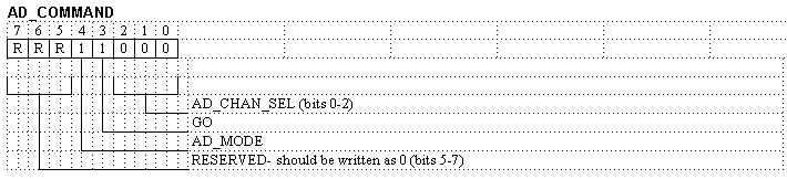
In the program listings 18H is loaded into AD_COMMAND. This sets up an 8-bit conversion on channel 0 starting now. Bits 0-2 select the channel for conversion. Bit 3 is responsible for starting the A/D conversion now as opposed to the HSO starting the conversion at some preset time. Bit 4 is used to select between 8 or 10 bit conversions. When using bit 4 a 1 represents an 8-bit conversion while a 0 represents a 10-bit conversion. The last 3 bits 5-7 are reserved and always should be written as 0.
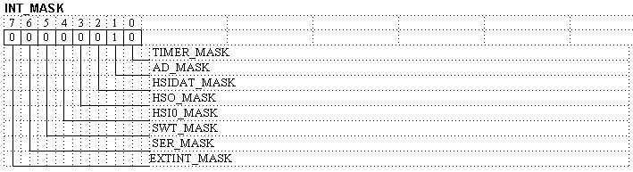
In the program listings 3 and 4, INT_MASK is loaded with 2H. Bit 1 is the only bit we need to worry about in this discussion of the A/D converter. By loading bit 1 with a value of 1 the A/D Conversion Complete interrupt is enabled. When this interrupt, INT01, occurs program flow is altered and the microcontroller will vector to memory location 2002H.
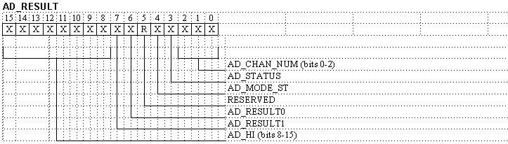
AD_RESULT is composed of a high byte and a low byte. Bits 0-2 hold the channel number that was used for the conversion. Bit 3 indicates the conversion status. If this bit is set then a conversion is in progress otherwise a 0 shows that the A/D converter is idle. If Bit 4 holds a 1 then an 8-bit conversion has taken place else a 0 shows that a 10-bit conversion has been done. Bit 5 is reserved and should always have 0 written to it even though it is rare that AD_RESULT is ever written to. Bits 6 and 7 hold the two least significant bits of a 10 bit conversion. Bits 8-15 hold the 8 most significant bits of the A/D conversion.
Programming the A/D Converter
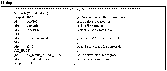
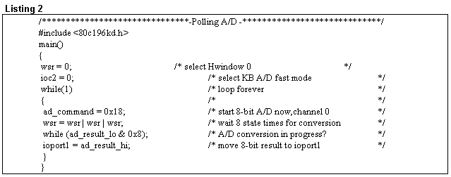
There are two different ways of checking for an end of conversion on the 8XC196KC/KD. One way of checking is to constantly monitor the status of bit 3 in AD_RESULT. This method gets the job done, but chews up sometimes costly CPU cycles. This method is demonstrated in program listings 1 and 2. Program listing 1 is written in ASM196(assembly code) while listing 2 is written in C196(C-code). A more preferable way of checking for an end of conversion is to generate an interrupt when the conversion is done. This method is demonstrated in program listings 3 and 4. The second method is an efficient way to free up the CPU to do other important things. In the following text, polling and interrupt programming methods will be discussed.
POLLING: (program listings 1 and 2)
This section describes how to go about setting up registers and coding the A/D converter. The first SFR we should take a look at is the SP(Stack Pointer). The SP should be loaded with a value when programming in ASM196. In program listings 1 and 3 a value of 100H was used. If you use C196 some of the initialization is already done for you, so this step is not needed. When reading or writing to the SFRs it is always important to be sure that you are in the correct horizontal window or Hwindow. For example, in order to access IOC2 we should select Hwindow 0. We select this Hwindow by loading the WSR(Window Select Register) with 0. IOC2 is loaded with a value of 0 to select the KB compatible mode with fast conversion. Next we need to load the AD_COMMAND SFR(Special Function Register) with 18H. By loading the register with 18H, we will be enabling 8-bit conversions on channel 0, starting immediately. After the conversion has begun it is important to wait 8 state times for the conversion to take place. After the 8 state time delay we may safely begin polling bit 3 of the AD_RESULT(LO) to see if a conversion is still in progress. We will loop until bit 3 is clear. After we are satisfied that we have successfully completed the conversion we can move the result to the IOPORT1 SFR. On the Intel 8XC196KC/KD Evaluation boards and Project Builder boards, IOPORT1 drives an 8-bit LED bank. By viewing the LED bank we can continuously monitor the A/D conversion results.
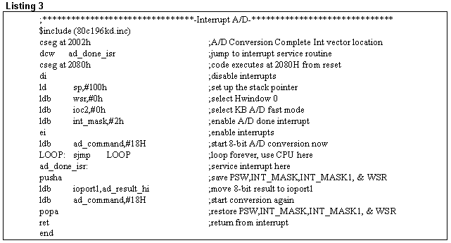
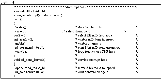
INTERRUPTS: (program listings 3 and 4)
Setting up the A/D converter to generate interrupts is similar to the polling procedure. The difference is when an interrupt is generated, the program flow is altered, unlike the polling situation. For example, the AD Conversion Complete interrupt causes the microcontroller to vector off to interrupt vector location 2002H. At that point a DCW command loads the location with the proper interrupt service routine location. (See program listing 3 for specifics.) In program listing 4, which accomplishes this task in C, setting up the interrupt vector location may seem more mysterious. When using C196, setting up the interrupt vector location is done by including the line #pragma interrupt(). In this case we set our ISR (Interrupt Service Routines) name equal to 1. Each interrupt in C196 is associated with a number. For instance, if a software timer interrupt is desired then the name of the ISR is assigned a value of 5. See your C196 user's manual for more information and the values associated with each interrupt.
Once we have set up our interrupt vector location we are ready to begin initialization. To begin coding, we should disable all interrupts to make sure they do not occur while we are initializing the A/D converter. Next we should load the stack pointer with 100H. In order to access the IOC2 SFR we should load WSR with 0, to select Hwindow 0. By loading IOC2 with 0 we are selecting the KB fast mode. We are now ready to load INT_MASK with 2H, this enables the A/D conversion complete interrupt. Now that we are done initializing we can enable the interrupts. To start the conversion process we load 18H into AD_COMMAND to start the 8-bit conversion on channel 0 now. While the conversion is taking place we will sit in an endless loop. This demonstrates that the processor is idle and capable of performing other tasks. For instance, this frees up resources to do things like FFTs (Fast Fourier Transforms) or other digital signal processing algorithms. At this point we need to set up the ISR. In assembly we should do a PUSHA upon entering the ISR and a POPA upon exiting the ISR for good measure. In C this is not necessary because it is already taken care of for us. Inside the ISR we load IOPORT1 with the contents of AD_RESULT(HI). This will display the 8-bit conversion result on the LED bank of an Intel 8XC196KC/KD Evaluation board or Project Builder board. Lastly we need to load AD_COMMAND with 18H to start the conversion process all over again.
PROGRAM LISTINGS: Program listings 1-4 can be found in the files, BTBEVAL.EXE for evaluation boards and, BTBDEVEL.EXE for Project Builder boards on the Intel Bulletin Board Service in the MCS(R) 96 Family / General section.
Legal Stuff © 1997 Intel Corporation
