AVOIDING DATA CORRRUPTION DURING WRITE AND RESET IN 8xC196 DESIGNS
If a RESET occurs during an external bus WRITE cycle, RAM data on the external bus may be corrupted. This TechBit describes a logic design that will alleviate the problem.
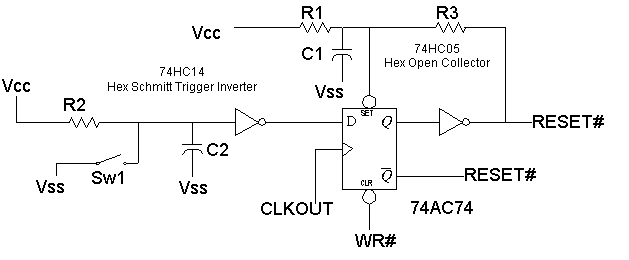
The following circuit will allow a manual RESET to occur at the rising edge of CLKOUT only if WR# is 'high' (inactive). If WR# is 'low' (active) then RESET# will stay 'high' (inactive). The 74HC14 and 74HC05 are usually already in the system so the only additional components are the 74AC74, R1, and C1.
For manual resets, the flip-flop will turn on at the next rising edge of CLKOUT unless WR# is low. If WR# is low, the flip-flop turn on will be delayed until the next rising edge of CLKOUT when WR# is not low. This may occur after any number of wait states. The R2*C2 time constant must be long enough for the normal RESET state times plus the maximum number of WRITE wait states.
Legal Stuff © 1997 Intel Corporation
