Abstract
This application brief explains how to program the MCS®96 device to operate the serial port in synchronous mode. A 4-bit multiplier which utilizes mode 0 with a port expansion circuit is presented.
Method of Operation
The serial port can be operated ina synchronous mode. This mode was intended for port expansion using shift registers. For example, the TXD pin is used to clock both input and output data on RXD. The data is always one byte in length. Whenever a write to the serial port buffer (SBUF) is performed a train of eight pulses is sent out TXD to clock the outgoing byte. Likewise, whenever SBUF is reached a train of eight pulses is sent out TXD to clock in the byte being read. See the synchronous serial mode timing diagram below:

Timing Considerations
All timings associated with the serial port are relative to TOSC. Therefore, the timings are fixed whether XTAL1 or T2CLK clocks the baud rate generator.
| TDVXH | Input Data Setup to Clock (TXD) Rising Edge. In other words, the data has to be valid at TDVXH before the next TXD pulse rises. |
| TQVXH | Output Data Setup to Clock (TXD) Rising Edge. The output bit will be valid before the rising edge of the next TXD pulse for TQVXH. |
| TXLXH | Serial Port Clock Falling Edge to Rising Edge. The low period for the TXD clock cannot be changed. For the 8X9X, TXLXH=4 TOSC+50. For KB, KC and KD, TXLXH=4 TOSC+50 or 2 TOSC+50 depending on the baud rate register value. |
NOTE: See the A.C. Characteristics in the datasheets for the timing specifications.
Setting Up the Control Registers

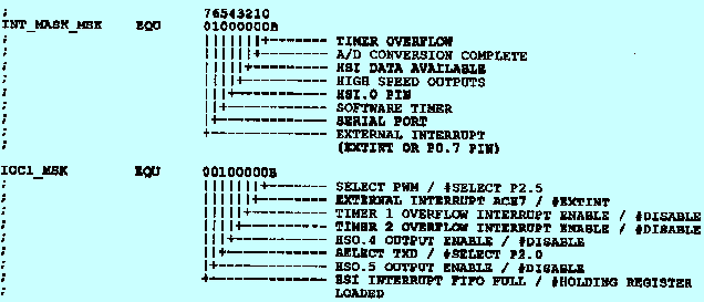
There are a few control registers that need to be utilized for mode 0 operation. First, since TXD is shared on the same pin as P2.0, we need to select the TXD function of that pin. This is accomplished setting bit 5 in IOC1 (16H).

In order to set the serial port to operate in mode 0, the serial port control register (sp_con11H) needs to be initialized. Bits 0 and 1 set the mode. Hence, setting them to zero enables mode 0. Also, in the sp_con is the receiver enable bit. Setting this bit (bit 3) enables the receiver (see RECEIVE).

The serial port status register (SP_STAT 11H) is located at the same address as sp_con. Writing to address 11H loads the serial port control register. Reading from 11H will read from the serial port status register (SP_STAT). Two status bits of importance are RI and TI. When set they indicate a receive completion or a transmit completion respectively. The RI and TI bits are cleared by reading SP_STAT.

NOTE: This interrupt is available on the 8X9X, KB, KC and KD.
There are two ways to monitor the status of the receiver and/or the transmitter. One is by polling the SP_STAT register (specifically RI and TI), the other is by using interrupts. RI is set whenever the receiver is done receiving one byte in mode 0. Likewise, TI is set whenever the transmitter has sent one byte in mode 0. If the SERIAL PORT interrupt bit in INT_MASK (09H) is inclusive OR of RI and TI. Hence, either RI or TI can cause a SERIAL PORT interrupt. Therefore, once the interrupt routine is entered, SP_STAT has to be tested to determine which interrupt (RI or TI) occured.
NOTE: These interrupts are available on the KB, KC, and KD-not on the 8X9X.
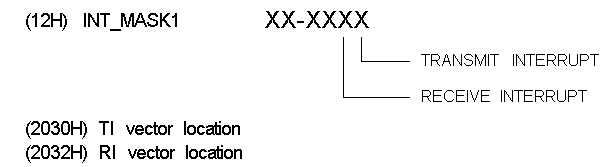
Additional interrupt vectors exist on the KB, KC and KD which make it easier to write code for the serial port. To interrupt on just the receive completion, the RI interrupt vector can be masked in. Similarly, the TI interrupt has a separate vector for transmit completion.
Receive
Reading the SP_STAT register always clears the RI bit and TI bit. If the RI bit is cleared while the RECEIVER ENABLE bit (bit 3 in SP_CON) is high, then another reception is started. Hence, it is possible to start another reception and overwrite the previous one. Therefore, don't poll SP_STAT to monitor the receiver. Use the serial port interrupt, the receive interrupt vector, or INT_PEND1 (KB, KC and KD) to test the RI bit for receive completion.
It is good programming practice to use the serial port interrupt or the RI interrupt for testing the RI. First, load the interrupt vector location with the appropriate ISR routine address. Next, enable the interrupt using either INT_MASK or INT_MASK1 depending on which interrupt is chosen. Now, enable interrupts using the EI instruction. Then, disable the receiver by clearing bit 3 in SP_CON (see above). Now the receiver is in a known state. To start a reception initiate a rising edge on the receiver enable bit (set bit 3 in SP_CON). When the service routine is entered, disable interrupts (i.e. PUSHF PUSHA) and read SBUF (07H) to obtain the received byte. To start another reception, clear the RI by reading SP_STAT. Then, enable interrupts (i.e. POPF or POPA), and return from the interrupt service routine. Clearing the RI bit while the receiver is enabled starts a reception and allows another serial port or receive interrupt to occur. To diable the receiver simply clear the RECEIVER ENABLE bit in SP_CON. See the programming example in the following pages.
Transmit
Transmitting a byte is much more straightforward. First, load SBUF (07H) with the byte to be transmitted. Two methods can be used to detect when transmit completion occurs: polling TI in SP_STAT, or using the serial port interrupt or TI interrupt (KB, KC and KD). Once again, using an interrupt to detect transmit complete is good programming practice.
To set up the transmit interrupt service routine, load the address of the ISR into either the serial port interrupt vector (200CH) or the TI interrupt vector (2030H). As with receive, mask in the appropriate interrupt using either INT_MASK or INT_MASK1. Enable interrupts with EI and, load SBUF with t byte to transmit.
When the interrupt service routine is entered disable interrupts (i.e. PUSHF or PUSHA). After the routine is executed another transmit can be started by loading SBUF again. Clear theTI bit in SP_STAT by reading SP_STAT. This action allows anotehr transmit or serial interrupt to occur. Enable interrupts before returning fromt the service routine (i.e. POPF or POPA). When the next transmit is done, another interrupt occurs (serial or transmit).
Example Using Mode 0
A programming example is included to demonstrate most of the above procedures for implementing mode 0. An evaluation board was used in conjunction with an I/O port expansion circuit to test out the following code. The program reads in one byte from an external shift register. Then, it multiplies the lower nibble by the upper nibble. The product is transmitted to another external shift register and is displayed on LEDs. The largest product is only OE1H which is OFH x OFH.
Hardware
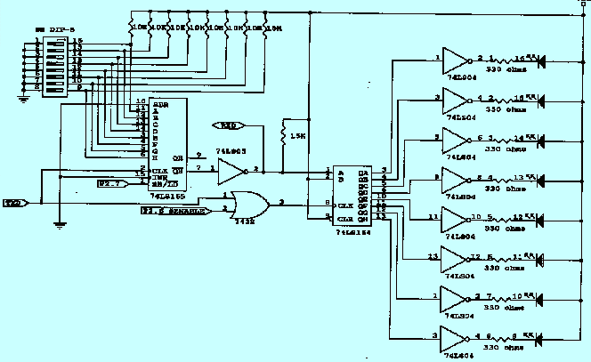
The schematic for this example is pictured in figure 1. The byte read is generated by a DIP switch attached to a parallel-in and serial-out register (74LS165). The output display is simply eight LEDs. The clock (TXD) is used to clock the parallel-in and serial-out shift register (74LS165). This (74LS165) register has two modes: a shift mode and a load mode. When, the transmit part of the circuit is activated, the 74LS165 is put into LOAD mode so the transmit shift register is not interfered with. To enable the transmit circuit, the TXD clock is gated to the 74LS164 (serial-in parallel out). The transmit circuit is enabled by the active low signal #ENABLE. The RXD line is used for receving and transmitting.
Inverter
The inverter (74LS05) has an open-collector output. A weak (15K) pull-up is used at the output. The purpose of the weka pull-up is so the RXD (when used as an output) can drive the data on RXD high low. If a regular inverter were used, then contention would exist between RXD (when used as an output) and the inverter output. Notice that the input inverter is QH#, hence the output of the inverter is the actual data QH.
OR Gate
The OR gate is a switch for the TXD clock. TXD is at one input. The other input is the ENABLE# (from P2.6). When the ENABLE# line is low, TXD passes freely through the OR gate. However, when ENABLE# is high, the output of the OR gate is always high. As a result there are no transitions at the output of the OR gate and the 74LS164 is not clocked.
DIP Switch
The DIP switch is weakly pulled high (switch off) and strongly driven low (switch on).
Software
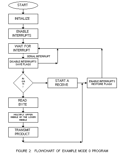
See the program listing for the software part of this example. Only the serial port interrupt is used in this example. Hence, this program is compatible with the 8X9XBH, KB, KC and KD. The flow chart in figure 2 below illustrates the algorithm.
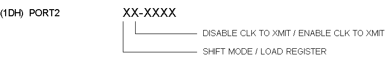
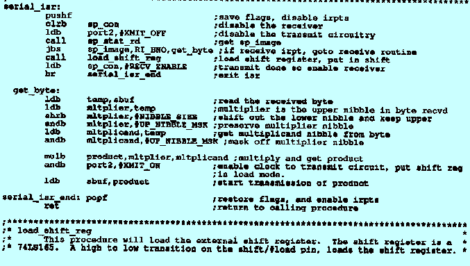
Now, the firts receive is started. The shift register must be loaded with the DIP switch byte. Hence, procedure is called to load the shift register and to set the register to shift mode. Port 2 is used to output control signals to the shift register and the transmit enable gate. Clearing P2.7 loads the register. Setting P2.7 puts the register in shift mode. Furthermore, to allow TXD to clock the transmit shift register P2.6 must be cleared. Setting P2.6 disables the TXD clock to the transmit shift register. Port 2 is diagrammed below:
The next step in starting a receive in this example is to disable the clock to the transmit circuit (see above). P2.6 is set by performing a logical OR. Next, mode 0 is selected and the receiver is disabled clearing all bits in SP_CON. Now, a rising edge on the REN bit is initiated by setting bit 3 in SP_CON. Finally, SP_STAT is cleared by reading it. Note that a special procedure was used to clear SP_STAT. This routine only needs to be called for the 8X9XBH (see techbit MC3391). The KB, KC and KD can simply do a LDB, temp, SP_STAT.
The foreground loop is entered until an interrupt occurs. There is only one interrupt routine - the serial port interrupt service routine. The first step in an interrupt routine is to disable other interrupts and save the flags. Next, the receiver is disabled by clearing SP_CON. Then, the TXD clock to the transmit circuitry is disabled by setting P2.6. The completion bits RI and TI are cleared (call SP_STAT_rd) to allow for the next interrupt. SP_IMAGE is returned from the SP_STAT_rd procedure. SP_IMAGE contains the status of the serial port upon entry into the service routine. The RI bit is tested in SP_IMAGE for receive completion.
If I receive just finished, then a transmit is initiated. First, the received byte is read in. Then, the nibbles are multiplied. The TXD clock to the transmit circuitry is enabled and the transmit is initiated.
Now, if a transmit caused the interrupt then, a receive is started. First, the external shift register is loaded by calling "load_shift_reg". Then, the receiver is enabled. A rising edge on REN starts another reception. The RI bit has already been cleared because sp_stat_rd was called. Hence, when the interrupt service routine is exited, the POPF enables interrupts and allows for the receive interrupt to occur.
Once again, the foreground loop is entered to await another interrupt.
Title: Mode 0 demonstration
Author: Richard N. Evans
Date: March 11, 1992
Description:
This program demonstrates the receive and transmit functions of mode 0. The following program is tailored for the 8X9XBH, 80C196KB, and 80C196KC running at 12MHz.
The code continually reads a byte from the receive buffer. It then multiplies the upper nibble by the lower nibble. Then, it outputs the product via the transmit buffer. The product is one byte in length.
One interrupt routine is necessary. The serial port interrupt is used. Once entered, either a receive or transmit is executed. If a receive done cause the interrupt, then the nibbles are multiplied and the product is transmitted. However, if a transmit done caused the interrupt, then receive is initiated.

serial isr
This routine services the serial port interrupt. If a receive or transmit is done, then the RI and TI bits get set and this routine is vectored to.
If a receive caused the interrupt, then the byte is read. The lower and upper nibbles are multiplied together. Finally, the product is written to the serial buffer which initiates a transmit.
If a transmit caused the interrupt, then that means a product was just written out the RXD pin. So, a receive is initiated to get the next byte.
INPUT: sbuf
OUTPUT: product, mltplier, mltplicand, port2, sbuf, sp_image
CHANGED: temp, sp_con, sp_stat, (plus OUTPUT)


© Intel Corporation, 1992

Legal Stuff © 1997 Intel Corporation