Rev. 1.0 (6/28/94)
Because of the small form factor, low pin-count package used for the Intel 80386EX processor, most peripheral pins have two functions associated with them, selectable via internal configuration registers. Many peripheral functions may be implemented internally or externally. To make the process of configuring the device pins easier, this document describes potential conflicts and alternate configuration options.
Table 1 shows which functions on the EX microprocessor share device pins. Although some peripherals share device pins, many signals can also be connected internally. A black box indicates that the peripheral in question shares some package pins with the other peripheral. For example, SIO0 is shown as conflicting with I/O Ports 1, 2, and 3. This DOES NOT mean that using SIO0 prohibits use of the listed I/O Ports. This indicates that the peripherals share some package pins. For more detailed information on specific pins, see the specific peripheral section.
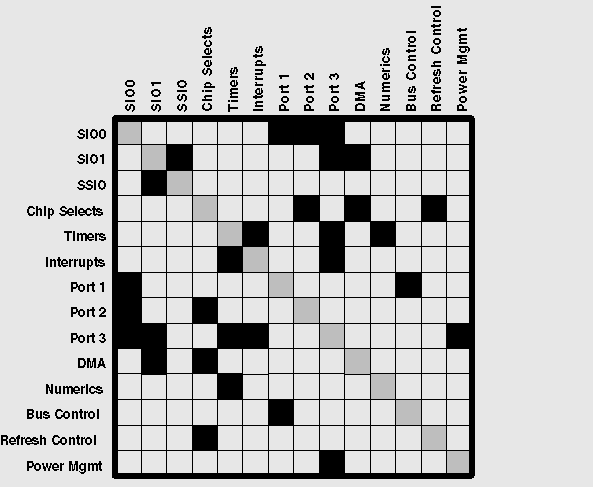
Table 1. Multiplexed Peripheral Functions
Each peripheral, its associated pins and their alternate functions are discussed, individually. Device Pin indicates the function chosen for a given device pin. Excluded Function indicates the alternate function of the given pin. Options for Excluded Functions describes other ways to implement the excluded function.. N/A means there is not internal support for the function in question. Configuration Registers lists the registers which must be programmed to configure a given device pin.
| Device Pin | Excluded Function | Options for Excluded Functions | Configuration Registers |
| RXD0 | P2.5 | Alternate Port Pin | P2CFG |
| TXD0 | P2.6 | Alternate Port Pin | P2CFG |
| CTS0# RTS0# DSR0# DTR0# DCD0# RI0# | P1.0 P1.1 P1.2 P1.3 P1.4 P2.7 | Alternate Port Pin Alternate Port Pin Alternate Port Pin Alternate Port Pin Alternate Port Pin Alternate Port Pin | P1CFG SIOCFG |
| COMCLK | P3.7 | Alternate Port Pin | SIOCFG, P3CFG |
Notes:
Even when the Port pins are configured for the peripheral function, the state of the peripheral pin can be read through the associated Port Pin State register. Modem signals are NOT individually selectable, they are either all routed to device pins, or all looped-back internally. When routed to the pins, at the pin multiplexer level, the modem signals can be individually selected. If the Port function is selected, the associated modem input signal is connected to its inactive level. For example, SIOCFG could be programmed to route all of the mode m signals to the pin multiplexers, but P1CFG can be programmed to configure one or more of the pins as a I/O Port function. In this situation, all pins selected to be I/O Port pins have the corresponding modem signal tied to Vcc, internally.
| Device Pin | Excluded Function | Options for Excluded Functions | Configuration Registers |
| RXD1 | DRQ1 | Internal DMA requests from: SIO1 Receive, SIO0 Transmit, SSIO Receive, and Timer 2. | N/A |
| TXD1 | DACK1* | DACK# is only valid for external DMA requests. A chip select can be used as a DACK#. | PINCFG |
| CTS1# RTS1# DSR1# DTR1# DCD1# RI1# | EOP# SSIOTX STXCLK SRXCLK DRQ0 SSIORX | N/A N/A N/A N/A Internal DMA requests from: SIO0 Receive, SIO1 Transmit, SSIO Transmit, and Timer 1. N/A | SIOCFG PINCFG |
| COMCLK | P3.7 | Alternate Port Pin | SIOCFG P3CFG |
Notes:
Modem signals are NOT individually selectable, they are either all routed to device pins, or all looped-back internally. When routed to the pins, at the pin multiplexer level, the modem signals can be individually selected. In the case of modem input CTS1#, it is tied to its inactive level when not selected at the pin multiplexer level. DSR1#, DCD1#, and RI1# are NOT automatically connected to their inactive state when they are not selected, they reflect the state of STXCLK, DRQ0, and SSIORX pins, respectively.
| Device Pin | Excluded Function | Options for Excluded Functions | Configuration Registers |
| SSIORX | RI1# | When using the SSIO functions, | SIOCFG |
| SSIOTX | RTS1# | SIO1 modem signals should be | PINCFG |
| SRXCLK | DTR1# | internally looped-back (see notes | |
| STXCLK | DSR1# | for Asynchronous Serial Port 1). |
Notes:
Modem signals are NOT individually selectable, they are either all routed to device pins, or all looped-back internally. When routed to the pins, at the pin multiplexer level, the modem signals can be individually selected. If the modem signals are routed to the pin multiplexers, and the SSIO function is selected at the pin level, the modem signals RTS1# and DTR1# are tied to Vcc, internally. RI1# and DSR1# are not automatically tied to Vcc, they follow the state of the SSIORX and STXCLK inputs, respectively. Therefore, it is recommended that the modem signals be internally looped back by programming SIOCFG appropriately.
| Device Pin | Excluded Function | Options for Excluded Functions | Configuration Registers |
| CS0# | P2.0 | Alternate Port Pin | P2CFG |
| CS1# | P2.1 | Alternate Port Pin | P2CFG |
| CS2# | P2.2 | Alternate Port Pin | P2CFG |
| CS3# | P2.3 | Alternate Port Pin | P2CFG |
| CS4# | P2.4 | Alternate Port Pin | P2CFG |
| CS5# | DACK0# | DACK# is only valid for external DMA requests. A chip select can be used as a DACK#. | PINCFG, DMACFG |
| CS6# | REFRESH# | BHE# and BLE# both high during a bus cycle also indicates a refresh cycle is in progress. | PINCFG |
| UCS# | None | N/A |
Notes:
Chip Selects are all individually selectable.
| Device Pin | Excluded Function | Options for Excluded Functions | Configuration Registers |
| TMROUT0 | P3.0 | Alternate Port Pin | P3CFG |
| TMRCLK0 | INT4 | N/A | TMRCFG |
| TMRGATE0 | INT5 | If TMRGATE0 is selected, INT5 must be internally tied to the SSIO interrupt. | TMRCFG |
| TMROUT1 | P3.1 | Alternate Port Pin | P3CFG |
| TMRCLK1 | INT6 | N/A | TMRCFG |
| TMRGATE1 | INT7 | N/A | TMRCFG |
| TMROUT2 TMRCLK2 TMRGATE2 | ERROR# PEREQ BUSY# | N/A | TMRCFG PINCFG |
Notes:
Timer 0 and Timer 1 signals are individually selectable. If the Timer Clock is not connected to a device input, internal clocks can be used. If the Timer Gate input is not connected to a device input, it can be internally connected to Vcc to enable counting. If Timer outputs are not connected to device pins, timers can be used
internally to generate DMA requests or interrupts. Timer 2 signals are not individually selectable. Either all Timer 2 functions or all Numerics functions are selected.
| Device Pin | Excluded Function | Options for Excluded Functions | Configuration Registers |
| INT0 | P3.2 | Alternate Port Pin | P3CFG |
| INT1 | P3.3 | Alternate Port Pin | P3CFG |
| INT2 | P3.4 | Alternate Port Pin | P3CFG |
| INT3 | P3.5 | Alternate Port Pin | P3CFG |
| INT4 | TMRCLK0 | TMRCLK0 must be tied to PSCLK internally to use Timer 0. | INTCFG TMRCFG |
| INT5 | TMRGATE0 | TMRGATE0 must be tied to Vcc internally to use Timer 0. | INTCFG TMRCFG |
| INT6 | TMRCLK1 | TMRCLK1 must be tied to PSCLK internally to use Timer 1. | INTCFG TMRCFG |
| INT7 | TMRGATE1 | TMRGATE1 must be tied to Vcc internally to use Timer 1. | INTCFG TMRCFG |
Notes:
All interrupt input pins are individually selectable. To minimize interrupt inputs required, Timer 0, Timer 1, Timer 2, SIO 0, SIO 1, SSIO, DMA and the Watchdog Timer are all supported by internal connections to the Interrupt Control Unit.
| Device Pin | Excluded Function | Options for Excluded Functions | Configuration Registers |
| P1.0 | DCD0# | When using the P1.0-1.4 functions, | P1CFG |
| P1.1 | RTS0# | the SIO0 modem signals can be | SIOCFG |
| P1.2 | DTR0# | looped-back internally. Otherwise | |
| P1.3 | DSR0# | they are tied to their inactive level. | |
| P1.4 | RI0# | ||
| P1.5 | LOCK# | N/A | P1CFG |
| P1.6 | HOLD | DMA Cascade Mode | P1CFG |
| P1.7 | HLDA | DMA Cascade Mode | P1CFG |
Notes:
All Port 1 pins are individually selectable (allowing implementation of a subset of a full modem interface). Port 1.6 and Port 1.7 are typically selected together as HOLD typically requires HLDA. SIO0 modem signals are only tied to Vcc, internally if they are routed to the pin multiplexers and the I/O Port function is selected.
| Device Pin | Excluded Function | Options for Excluded Functions | Configuration Registers |
| P2.0 | CS0# | Even if a chip select is not | P2CFG |
| P2.1 | CS1# | connected to a device output, it can | P2CFG |
| P2.2 | CS2# | still be used to generate wait-states, | P2CFG |
| P2.3 | CS3# | READY#, LBA#, and BS8#. | P2CFG |
| P2.4 | CS4# | P2CFG | |
| P2.5 | RXD0 | Alternate Serial Channel | P2CFG |
| P2.6 | TXD0 | Alternate Serial Channel | P2CFG |
| P2.7 | CTS0# | If SIO0 modem signals are not looped-back internally, selecting P2.7 pulls CTS0# to its inactive level. | P2CFG SIOCFG |
| Device Pin | Excluded Function | Options for Excluded Functions | Configuration Registers |
| P3.0 | TMROUT0 | Timer 0 can be used to generate interrupts internally. | P3CFG |
| P3.1 | TMROUT1 | Timer 1 can be used to generate interrupts or DMA requests internally. | P3CFG |
| P3.2 | INT0 | N/A | P3CFG |
| P3.3 | INT1 | N/A | P3CFG |
| P3.4 | INT2 | N/A | P3CFG |
| P3.5 | INT3 | N/A | P3CFG |
| P3.6 | PWRDOWN | N/A | P3CFG |
| P3.7 | COMCLK | SIO0 and SIO1 can be clocked internally with SERCLK. | P3CFG |
| Device Pin | Excluded Function | Options for Excluded Functions | Configuration Registers |
| DRQ0 | DCD1# | If SIO1 modem signals are not | DMACFG, SIOCFG |
| EOP# | CTS1# | looped-back internally, CTS1# is tied to its inactive level, but DCD1# reflects DRQ0. | |
| DACK0# | CS5# | Alternate Chip Select or it can still be used to generate wait-states, READY#, LBA#, and BS8#. | DMACFG, PINCFG |
| DRQ1 | RXD1 | Alternate Serial Channel | DMACFG |
| DACK1# | TXD1 | Alternate Serial Channel | DMACFG, PINCFG |
| Device Pin | Excluded Function | Options for Excluded Functions | Configuration Registers |
| ERROR# PEREQ BUSY# | TMROUT2 TMRCLK2 TMRGATE2 | TMR2GATE is tied to Vcc internally. TMRCLK2 can be tied to PSCLK internally. Timer 2 can be used to generate interrupts or DMA requests internally. | TMRCFG PINCFG |
Notes:
Numerics signals are not individually selectable. If Timer2 functions are selected at device pins, all numeric interface signals are tied to their inactive state.
| Device Pin | Excluded Function | Options for Excluded Functions | Configuration Registers |
| LOCK# | P1.5 | Alternate Port Pin | P1CFG |
| HOLD | P1.6 | Alternate Port Pin | P1CFG |
| HLDA | P1.7 | Alternate Port Pin | P1CFG |
Notes:
Bus Control signals are individually selectable. HOLD and HLDA are typically selected together, but this is not required. Even when the non-port function is selected, the state of the peripheral signal can be monitored by reading the Port Pin State register.
| Device Pin | Excluded Function | Options for Excluded Functions | Configuration Registers |
| REFRESH# | CS6# | Alternate Chip Select or it can still be used to generate wait-states, READY#, LBA#, and BS8#. | PINCFG |
| Device Pin | Excluded Function | Options for Excluded Functions | Configuration Registers |
| PWRDOWN | P3.6 | Alternate Port Pin | P3CFG |
Legal Stuff © 1997 Intel Corporation
