![[INTEL NAVIGATION HEADER]](../../PIX/HEADER.GIF)
Features of Differential Delay Line used on the Embedded Ultra Low Power Intel486 Processor
by Shankar Gupta
APC Design Engineering
Abstract
For certain applications, it is desirable for embedded processors to perform at high frequencies, while consuming much lower amounts of power. Traditional analog Phase Locked Loops (PLL's) are used by Intel486(TM) processors to clock internal circuitry at a 1x or 2x multiple of external clock (CLK) input. The PLL's start up time is extremely long. Consequently the processor's power consumption is also high for many embedded applications. The embedded Ultra Low Power (ULP) Intel486 processor uses a newly designed Differential Delay Line (DDL), to implement internal clocking. Features of such a DDL are described in this paper.
Introduction
Intel486 processors require a CLK input, that provides the fundamental timing and internal operating frequency. Refer to the Intel486 Microprocessor Family handbook for CLK specifications. Depending upon the processor specifications, an Intel486 processor core can operate at a single (1X mode), double (2X mode) or triple (3X mode) multiple of the external bus and CLK frequency. Such internal frequency multiplication has been implemented by using traditional analog PLL circuits. However such PLL circuits can take a long time, upto a 1mS, to start up. The minimum voltage of operation (about 2V), and idle power consumption of the PLL is also very high for certain embedded applications. These problems are solved by the embedded ULP Intel486 processor by using a DDL. This mostly digital DDL which is capable of operation at 1.2V, allows a fast start up time of 8 clocks of CLK input. The embedded ULP Intel486 processor reduces power consumption by freezing clocks internally and by also allowing the processor clock to be stopped externally. Details of the clock freeze methodology to reduce power are described elsewhere, and not described in this paper. This paper describes the features of the DDL, that is used by the embedded ULP Intel486 processor, as part of the overall low power solution.
Description of DDL
The block diagram of the DDL is given by Fig. 1. It comprises of a Pulse Generator, Sequencer, Delay Line, Timing Comparator, Error Detector, Multiplexer and Phase Generator.
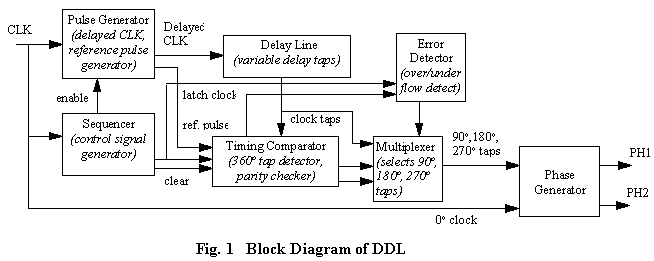
Pulse Generator
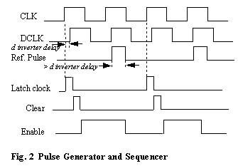
The Pulse Generator (PG) generates a clock signal (DCLK) that is simply the input CLK signal delayed by d number of inverters. Another reference pulse, wider than d inverter delay, is generated at every other rising edge of CLK. The reference pulse is used by the Timing Comparator. Fig. 2 describes the Pulse Generator outputs.
Sequencer
Fig. 2 describes how for every 2-cycle period of CLK, the sequencer generates a Clear and Enable control signal. Clear resets the Timing Comparator, while the Enable enables the Reference Pulse of the PG. A latch clock signal for the Timing Comparator and Error Detector is also generated.
Delay Line
The DCLK is fed through a series Delay Line (DL) chain of n inverters. Therefore n number of clock pulses, each separated by one inverter delay are available. From these delayed clock pulses, another set of n number of delayed pulse taps, each being m (m<<n) inverter delay wide, are extracted.
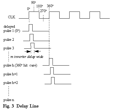
Depending upon the period of CLK, one of the n pulses, say pulse h, is exactly 1 cycle delayed. This is the 360 hit case. Fig. 3 describes the generation of the delay pulses, an example 0 pulse and a 360 hit case.
Timing Comparator
The Timing Comparator (TC) combines about one half of the n delayed pulses together with the reference pulse generated by PG. It determines which of the (total of n/2) delayed pulses is exactly 1 clock cycle delayed as compared to CLK. This is the 360delayed tap and forms the basis for determining the 90, 180 and 270 taps. Fig. 3 describes the 0, 90, 180 and 270points of the CLK. The slowest frequency the DL can correctly resolve is the case when the CLK time period is exactly equal to n inverter delay. In this case the 90, 180 and 270 points are the n/4, n/2 and 3n/4 delayed clock taps from the DL. In case of higher CLK frequencies, when the CLK time period is less than the delay produced by n/2 inverters, more than one 360 hit case will be found by the timing comparator. In such cases only the first occurrence is considered important and the rest are ignored. The TC also generates a parity signal in case an odd number tap happens to be the 360 hit case.
Error Detector
The Error Detector generates an overflow signal in case the TC is unable to locate a 360 hit case for a low frequency CLK. This is the case when the CLK time period is greater than the delay produced by n inverters. In such a situation the 90, 180 and 270 points are calculated based on the slowest valid frequency the DL can handle. In slow frequency cases, the DDL functions but may produce non 50% duty cycle outputs. A timing diagram for the overflow case is shown later. The case of CLK which is faster for the DL to handle occurs when every one of the delayed pulses processed by the TC produces a 360 hit case. Theoretically, this is the case when the CLK time period is smaller than one inverter delay. In the practical case of this DDL, a CLK time period smaller than a few inverter delays is actually the DDL's limitation. This fast frequency case causes an underflow signal. The DDL will not produce valid PH1 and PH2 signals at frequencies that generate an underflow signal.
Multiplexer
The information about the 360 tap, together with all of the n delayed pulses from the Delay Line is fed into the Multiplexer block. If the 360 point (h) is an even number, then the 90, 180 and 270 points are calculated as the taps that are one fourth, one half and three fourth of h respectively. These outputs are fed into the Phase Generator for final clock generation. In case the 360 hit case (h) is odd, the h-1 point is assumed to be the 360 point. In this case MOS capacitors are turned on to compensate one inverter delay to the 90, 180 and 270 outputs, as the outputs go active.
Phase Generator
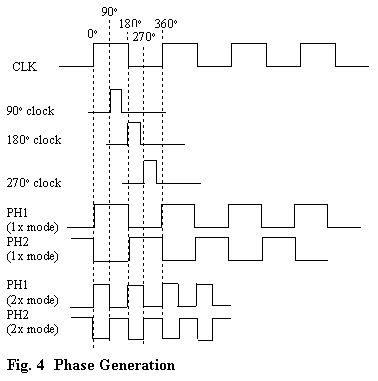
The Phase Generator (PHG) processes the CLK (0 point) and the 90, 180 and 270 outputs from the Multiplexer, to produce the PH1 and PH2 clocks. Based on the 0 and the 180 points, the PH1 and PH2 signals are generated in the single clock (1X) mode. Based on the 0, 90, 180 and 270 outputs, the PH1 and PH2 signals are generated in the double clock (2X) mode. Fig. 4 describes the inputs and outputs of the PHG. The 90, 180 and 270 outputs determined during the first CLK cycle are preserved and reused during the second CLK cycle. As mentioned in Fig. 2, the Clear signal then resets the TC circuitry and the process to determine the 90, 180 and 270 output points, starts all over again.
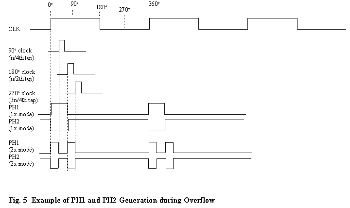
An example of how the DDL handles a case of very slow CLK frequency is described by Fig. 5. The time period of CLK is greater than the delay produced by the n inverter chain and the overflow signal is generated. Consequently the 90, 180 and 270 points are chosen to be the n/4, n/2 and 3n/4 delayed clock taps from the DL. Notice that in the 1X mode case, while the PH1/PH2 time period is same as that of CLK, the duty cycle is not 50%. Similarly for the 2x mode case the duty cycle of the second PH1/PH2 clock combination is not 50%. In both the 1x and 2x modes since PH1 is short, PH2 is extended to fill-up the remaining time and synchronize with the CLK period.
Operation Details of the DDL
The operating features of the DDL are summarized by Table 1. In particular, the DDL operates within the CLK period stability specification of ±250ps.
Table 1
| Parameter |
Value |
| Vcc Range |
1.2Volts (@12.5MHz, 90°C case temperature 176 tqfp package)
~ 6.0Volts (@66MHz, 90°C case temperature 176 tqfp package) |
| CLK Range |
0 ~ 33MHz (1x mode, 2.3V ~ 3.8V)
0 ~ 25MHz (2x mode, 2.8V ~ 3.8V) |
| Power Consumption |
13mA (maximum @ 3.8V, 33MHz CLK)
5µA (@ 3.8V, 0MHz CLK) |
| Clocks spent for startup |
8 |
| to stop |
1 |
Allowable input variation for Vcc,
temperature and clock |
1200mV/µs, 120C/µs, 250ps/clock |
Benefits of using DDL
To conserve power, the embedded ULP Intel486 processor depends upon the fast clock startup and stop times of the DDL. At 33 MHz for example, the DDL startup time is 240ns while the stop time is 30ns. Traditional PLL circuits need about 1mS of startup and stop times each. The mostly digital DDL circuitry itself consumes low power 5 µA @ 3.8V when idle as compared to about 100 µ A for traditional PLL circuits. The DDL therefore plays an important role in helping reduce overall power consumption. The DDL meets the traditional CLK period stability specification of ±250ps. While ultra low voltage operation at 1.2V has been demonstrated by the embedded ULP Intel486 processor, it is unclear if traditional PLL circuits would perform at these low voltages on the same process technology.
For on-demand low power applications such as mobile phones, when compared to traditional PLL designs, the DDL consumes lower power (5 µA vs. 100 µA @ 3.8V), and also allows significantly faster power up times (240ns vs. 1mS @ 33MHz).
Conclusion
The embedded ULP Intel486 processor uses a DDL circuit for internal clock generation. Its operation and operating ranges have been described in this paper. The benefit to system designers is that the DDL consumes far less power during power-up/power-down cycles than designs utilizing traditional PLL circuits, thus producing significant power savings for on-demand applications.
References
1. Intel486(TM) Microprocessor Family Handbook, September 1994.
2. Novel Clock Generator Differential Delay Line Overview Rev. 1.2, 1/12/94, Japan Design Center.
3. Novel Clock Generator Differential Delay Line, Design Report Rev. 1.0, 2/25/94, Japan Design Center.
Legal Stuff © 1997 Intel Corporation
