![[INTEL NAVIGATION HEADER]](../../PIX/HEADER.GIF)
80C18xEB Pinout and Packaging Information
80C186EB Pinout
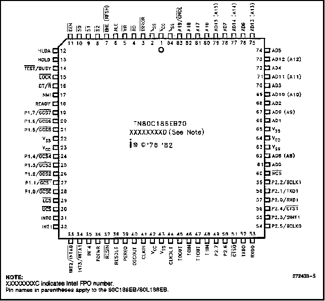
Tables 4 and 5 list the 80C186EB pin names with package location for the 84-pin Plastic Leaded Chip Carrier (PLCC) component. Figure 5 depicts the complete 80C186EB pinout (PLCC package) as viewed from the tip side of the component (i.e., contacts facing down).
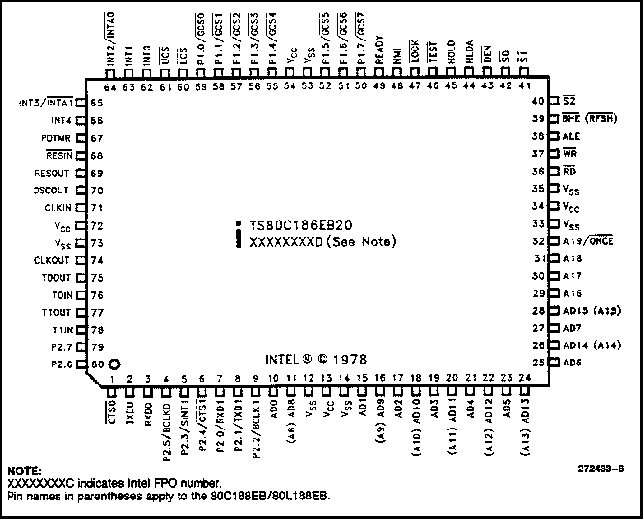
Tables 6 and 7 list the 80C186EB pin names with package location for the 80-pin Quad Flat Pack (EIAJ) component. Figure 6 depicts the complete 80C186EB/80C188EB (QFP package) as viewed from the top side of the component (i.e., contacts facing down).
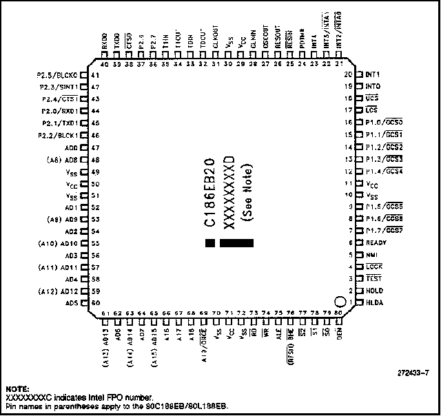
Tables 8 and 9 list the 80C186EB/80C188EB pin names with the package location for the 80-pin Quad Flat Pack (SQPF) component. Figure 7 depicts the complete 80C186EB/80C188EB (SQFP) as viewed from the top side of the component (i.e., contacts facing down).
| Table 4. PLCC Pin Names with Package Location |
| Address/Data Bus |
| Name | Location |
AD0
AD1
AD2
AD3
AD4
AD5
AD6
AD7
AD8(A8)
AD9(A9)
AD10(A10)
AD11(A11)
AD12(A12)
AD13(A13)
AD14(A14)
AD15(A15)
A16
A17
A18
A19/ONCE |
61
66
68
70
72
74
76
78
62
67
69
71
73
75
77
79
80
81
82
83 |
|
| Bus Control |
| Name | Location |
ALE
RHE(RFSH)
S0
S1
S2
RD
WR
READY
DEN
DT/R
LOCK
HOLD
HLDA
|
6
7
10
9
8
4
5
18
11
16
15
13
12 |
| Power
| | Name | Location |
Vss
Vcc |
2,22,43
63,65,84
1,23
42,64 |
|
| Processor Control
| | Name | Location |
RESIN
RESOUT
CLKIN
OSCOUT
CLKOUT
TEST/BUSY
NCS(N.C.)
PEREQ(N.C.)
ERROR(N.C.)
PDTMR
NMI
INT0
INT1
INT2/INTA0
INT3/INTA1
INT4 | 37
38
41
40
44
14
60
39
3
36
17
31
32
33
34
35 |
|
| I/O
| | Name | Location |
UCS
LCS
P1.0/GCS0
P1.1/GCS1
P1.2/GCS2
P1.3/GCS3
P1.4/GCS4
P1.5/GCS5
P1.6/GCS6
P1.7/GCS7
T0OUT
TOIN
T1OUT
T1IN
RXD0
TXD0
P2.5/BCLK0
CTS0
P2.0/RXD1
P2.1/TXD1
P2.2/BCLK1
P2.3/SINT1
P2.4/CTS1
P2.6
P2.7 | 30
29
28
27
26
25
24
21
20
19
45
46
47
48
53
52
54
51
57
58
59
55
56
50
49
|
|
Note:
Pin names in parentheses apply to the 80C188EB/80L188EB
| Table 5. PLCC Package Locations with Pin Names
|
| Location | Name |
1
2
3
4
5
6
7
8
9
10
11
12
13
14
15
16
17
18
19
20
21
|
Vss
Vcc
ERROR(N.C.)
RD
WR
ALE
BHE(RFSH)
S2
S1
S0
DEN
HLDA
HOLD
TEST/BUSY
LOCK
DT/R
NMI
READY
P1.7/GCS7
P1.6/GCS6
P1.5/GCS5 |
|
| Location | Name |
22
23
24
25
26
27
28
29
30
31
32
33
34
35
36
37
38
39
40
41
42 |
Vss
Vcc
P1.4/GCS4
P1.3/GCS3
P1.2/GCS2
P1.1/GCS1
P1.0/GCS0
LCS
UCS
INT0
INT1
INT2/INTA0
INT3/INTA1
INT4
PDTMR
RESIN
RESOUT
PEREQ(N.C.)
OSCOUT
CLKIN
Vcc |
|
| Location | Name |
43
44
45
46
47
48
49
50
51
52
53
54
55
56
57
58
59
60
61
62
63 |
Vss
CLKOUT
T0OUT
T0IN
T1OUT
T1IN
P2.7
P2.6
CTS0
TXD0
RXDO
P2.5/BLCK0
P2.3/SINT1
P2.4/CTS1
P2.0/RXD1
P2.1/TXD1
P2.2/BLCK1
NCS(N.C.)
AD0
AD8(A8)
Vss |
|
| Location | Name |
64
65
66
67
68
69
70
71
72
73
74
75
76
77
78
79
80
81
82
83
84 |
Vcc
Vss
AD1
AD9(A9)
AD2
AD10(A10)
AD3
AD11(A11)
AD4
AD12(A12)
AD5
AD13(A13)
AD6
AD14(A14)
AD7
AD15(A15)
A16
A17
A18
A19/ONCE
Vss |
|
Note:
Pin names in parentheses apply to the 80C188EB/80L188EB.
Figure 4. 84-Pin Plastic Leaded Chip Carrier Pinout Diagram.
| Table 6. QFP Pin Names with Package Location |
| Address/Data Bus |
| Name | Location |
AD0
AD1
AD2
AD3
AD4
AD5
AD6
AD7
AD8(A8)
AD9(A9)
AD10(A10)
AD11(A11)
AD12(A12)
AD13(A13)
AD14(A14)
AD15(A15)
A16
A17
A18
A19/ONCE |
10
15
17
19
21
23
25
27
11
16
18
20
22
24
26
28
29
30
31
32 |
|
| Bus Control |
| Name | Location |
ALE
BHE(RFSH)
S0
S1
S2
RD
WR
READY
DEN
LOCK
HOLD
HLDA
|
38
39
42
41
40
36
37
49
43
47
45
44 |
| Power
| | Name | Location |
Vss
Vcc |
12,14,33
35,53,73
13,34
54,72 |
|
| Processor Control
| | Name | Location |
RESIN
RESOUT
CLKIN
OSCOUT
CLKOUT
TEST
PDTMR
NMI
INT0
INT1
INT2/INTA0
INT3/INTA1
INT4 |
68
69
71
74
46
67
48
62
63
64
68
66 | |
I/O
| Name | Location |
UCS
LCS
P1.0/GCS0
P1.1/GCS1
P1.2/GCS2
P1.3/GCS3
P1.4/GCS4
P1.5/GCS5
P1.6/GCS6
P1.7/GCS7
T0OUT
TOIN
T1OUT
T1IN
RXD0
TXD0
P2.5/BCLK0
CTS0
P2.0/RXD1
P2.1/TXD1
P2.2/BCLK1
P2.3/SINT1
P2.4/CTS1
P2.6
P2.7 |
61
60
59
58
57
56
55
52
51
50
75
76
77
78
3
2
4
1
7
8
9
5
6
80
79
| |
|
Note:
Pin names in parentheses apply to the 80C188EB/80L188EB
| Table 7. QFP Package Locations with Pin Names
|
| Location | Name |
1
2
3
4
5
6
7
8
9
10
11
12
13
14
15
16
17
18
19
20 |
CTS0
TXD0
RXD0
P2.5/BCLK0
P2.3/SINT1
P2.4/CTS1
P2.0/RXD1
P2.1/TXD1
P2.2/BCLK1
AD0
AD8(A8)
Vss
Vcc
Vss
AD1
AD9(A9)
AD2
AD10(A10)
AD3
AD11(A11) | |
| Location | Name |
21
22
23
24
25
26
27
28
29
30
31
32
33
34
35
36
37
38
39
40 |
AD4
AD12(A12)
AD5
AD13(A13)
AD6
AD14(A14)
AD7
AD15(A15)
A16
A17
A18
A19/ONCE
Vss
Vcc
Vss
RD
WR
ALE
BHE(RFSH)
S2 |
|
| Location | Name |
41
42
43
44
45
46
47
48
49
50
51
52
53
54
55
56
57
58
59
60 |
S1
S0
DEN
HLDA
HOLD
TEST
LOCK
NMI
READY
P1.7/GCS7
P1.6/GCS6
P1.5/GCS5
Vss
Vcc
P1.4/GCS4
P1.3/GCS3
P1.2/GCS2
P1.1/GCS1
P1.0/GCS0
LCS |
|
| Location | Name |
61
62
63
64
65
66
67
68
69
70
71
72
73
74
75
76
77
78
79
80 |
UCS
INT0
INT1
INT2/INTA0
INT3/INTA1
INT4
PDTMR
RESIN
RESOUT
OSCOUT
CLKIN
Vcc
Vss
CLKOUT
T0OUT
T0IN
T1OUT
T1IN
P2.7
P2.6
|
|
Note:
Pin names in parentheses apply to the 80C188EB/80L188EB.
Figure 5. Quad Flat Pack Pinout Diagram
| Table 8. SQFP Pin Functions with Location |
| AD Bus |
AD0
AD1
AD2
AD3
AD4
AD5
AD6
AD7
AD8(A8)
AD9(A9)
AD10(A10)
AD11(A11)
AD12(A12)
AD13(A13)
AD14(A14)
AD15(A15)
A16
A17
A18
A19/ONCE |
47
52
54
56
58
60
62
64
48
53
55
57
59
61
63
65
66
67
68
69 |
|
| Bus Control |
ALE
BHE(RFSH)
S0#
S1#
S2#
RD#
WR#
READY
DEN#
LOCK#
HOLD
HLDA
| 75
76
79
78
77
73
74
6
80
4
2
1 | |
| Processor Control
| RESIN#
RESOUT
CLKIN
OSCOUT
CLKOUT
TEST#/BUSY
NMI
INT0
INT1
INT2/INTA0#
INT3/INTA1#
INT4
PDTMR |
25
26
28
27
31
3
5
19
20
21
22
23
24 |
| Power and Ground
| Vcc
Vss |
11,29
50,71
10,30,49
51,70,72 |
|
I/O
UCS#
LCS#
P1.0/GCS0#
P1.1/GCS1#
P1.2/GCS2#
P1.3/GCS3#
P1.4/GCS4#
P1.5/GCS5#
P1.6/GCS6#
P1.7/GCS7#
P2.0/RXD1
P2.1/TXD1
P2.2/BCK1
P2.3/SINT1
P2.4/CTS#
P2.5/BCLK0
P2.6
P2.7
CTSO#
TXD0
RXT0
T0IN
T1IN
T0OUT
T1OUT |
18
17
16
15
14
13
12
9
8
7
44
45
46
42
43
41
37
36
38
39
40
33
35
35
34
| |
|
| Table 9. SQFP Pin Locations with Pin Names
|
1
2
3
4
5
6
7
8
9
10
11
12
13
14
15
16
17
18
19
20 |
HLDA
HOLD
TEST#
LOCK#
NMI
READY
P1.7/GCS7#
P1.6/GCS6#
P1.5/GCS5#
Vss
Vcc
P1.4/GCS4#
P1.3/GCS3#
P1.2/GCS2#
P1.1/GCS1#
P1.0/GCS0#
LCS#
UCS#
INT0
INT1 | |
21
22
23
24
25
26
27
28
29
30
31
32
33
34
35
36
37
38
39
40 |
INT1/INTA0#
INT3/INTA1#
INT4
PDTMR
RESIN#
RESOUT
OSCOUT
CLKIN
Vcc
Vss
CLKOUT
T0OUT
T0IN
T1OUT
T1IN
P2.7
P2.6
CTS0#
TXD0
RXD0 |
|
41
42
43
44
45
46
47
48
49
50
51
52
53
54
55
56
57
58
59
60 |
P2.5/BCLK0
P2.3/SINT1
P2.4/CTS1#
P2.0/RXD1
P2.1/TXD1
P2.2/BCLK1
AD0
AD9(A8)
Vss
Vcc
Vss
AD1
AD9(A9)
AD2
AD10(A10)
AD3
AD11(A11)
AD4
AD12(A12)
AD5 |
|
61
62
63
64
65
66
67
68
69
70
71
72
73
74
75
76
77
78
79
80 |
AD13(A13)
AD6
AD14(A14)
AD7
AD15(A15)
A16
A17
A18
A19/ONCE
Vss
Vcc
Vss
RD#
WR#
ALE
BHE#(RFSH#)
S2#
S1#
S0#
DEN#
|
|
Note:
Pin names in parentheses apply to the 80C188EB/80L188EB.
Figure 6. SQFP Package
Plastic Leaded Chip Carrier Package
Symbol List for Plastic Leaded Chip Carrier Family
|
Letter of Symbol | Description of Dimensions |
| A | Overall Height: Distance form seating plane to highest point of body |
| A1 | Distance from lead shoulder to seating plane |
| CP | Seating plane coplanarity |
| D/E | Overall package dimension |
| D1/E1 | Plastic body dimension |
| D2/E2 | Footprint |
| LT | Lead thickness |
| N | Total number of leads |
| Nd | Total number of leads on short side |
| Ne | Total number of leads on long side |
| TCP | Tweezing coplanarity |
Notes Rectangle Package:
1. All dimensions and tolerance conform to ANSI Y14.M-1982
2. Datum plan -H- located at top of mold parting line and coincidnet with top of lead, where lead exits plastic body.
3. Datums A-B and -D- to be determined where center leads exit plastic body at datum plane -H-.
4. To be determined at seating plane -C-
5. Dimensions D1 and E1do not include mold protrusion.
6. Pin 1 identifier is located within the defined zone.
7. These two dimensions determine maximum angle of the lead for centrain socket applications. If unit is intended to be socketed, it is advisable to review these dimensions with the socket supplier.
8. Nd denotes the number of leads on the two short sides of the package, one of which contains pin #1. Ne denotes the number of leads on the two long sides of the package.
9. Controlling dimension, inch.
10. All dimensions and tolerances include lead trim offset and lead plating finish.
11. Tweezing surface planarity is defined as the furthest any lead on a side may be from the datum. The datum is established by touching the outermost lead on that side and parallel to A-B OR -D-.
| Packaging Family Attributes |
| Category | Plastic Leaded Chip Carrier |
| Acronym | PLCC |
| Lead Configuration | Quad |
| Lead Counts | 28, 32, 44, 52, 68, 84 |
| Lead Finish | SolderPlate |
| Lead Pitch | 0.050" |
| Board Assembly Type | Socket and Surface Mount |
Notes:
1. Copper Alloy Leads.
2. Novalac Body.
3. Bake and dessicant packaging required.
| Family: Plastic Leaded Chip Carrier-Square (mm) |
| Symbol | 52 Lead |
68 Lead | 84 Lead |
| | Min | Max | Notes | Min | Max | Notes | Min | Max | Notes |
| A | 4.19 | 4.57 | | 4.19 |
4.83 | | 4.19 | 4.83 | |
| A1 | 2.29 | 3.05 | | 2.29 |
3.05 | | 2.29 | 3.05 | |
| D | 19.9 | 20.2 | | 25.0 |
25.3 | | 30.1 | 30.4 | |
| D1 | 19.1 | 19.2 | | 24.1 |
24.3 | | 29.2 | 29.4 | |
| D2 | 17.5 | 18.5 | | 22.6 | 23.6 | | 27.7 | 28.7 | |
| E | 19.9 | 20.2 | | 25.0 | 25.3 | | 30.1 | 30.4 | |
| E1 | 19.1 | 19.2 | | 24.1 | 24.3 | | 29.2 | 29.4 | |
| E2 | 17.5 | 18.5 | | 22.6 | 23.6 | | 27.7 | 28.7 | |
| N | 52 | | 68 | | 84 | |
| CP | 0.00 | 0.10 | | 0.00 | 0.10 | | 0.00 | 0.10 | |
| TCP | 0.00 | 0.10 | | 0.00 | 0.10 | | 0.00 | 0.10 | |
| LT | 0.23 | 0.38 | | 0.20 | 0.36 | | 0.20 | 0.36 | |
| Family: Plastic Leaded Chip Carrier-Square (inch) |
| Symbol | 52 Lead |
68 Lead | 84 Lead |
| | Min | Max | Notes | Min | Max | Notes | Min | Max | Notes |
| A | 0.165 | 0.180 | | 0.165 |
0.190 | | 0.165 | 0.190 | |
| A1 | 0.090 | 0.120 | | 0.090 |
0.120 | | 0.090 | 0.120 | |
| D | 0.785 | 0.795 | | 0.985 |
0.995 | | 1.185 | 1.195 | |
| D1 | 0.750 | 0.756 | | 0.950 |
0.958 | | 1.150 | 1.158 | |
| D2 | 0.690 | 0.730 | | 0.890 | 0.930 | | 1.090 | 1.130 | |
| E | 0.785 | 0.795 | | 0.985 | .0995 | | 1.185 | 1.195 | |
| E | 0.750 | 0.756 | | 0.950 | 0.958 | | 1.150 | 1.158 | |
| E2 | 0.690 | 0.730 | | 0.890 | 0.930 | | 1.090 | 1.130 | |
| N | 52 | | 68 | | 84 | |
| CP | 0.000 | 0.004 | | 0.000 | 0.004 | | 0.000 | 0.004 | |
| TCP | 0.000 | 0.004 | | 0.000 | 0.004 | | 0.000 | 0.004 | |
| LT | 0.009 | 0.015 | | 0.008 | 0.014 | | 0.008 | 0.014 | |
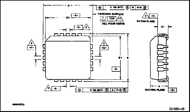
Figure 1. Principal Dimensions and Datums
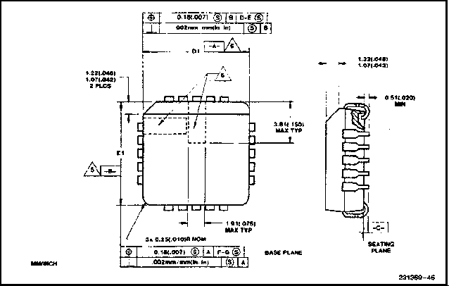
Figure 3. Terminal Details
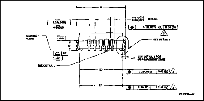
Figure 4A. Standard Package Bottom View (Tooling Option I.)
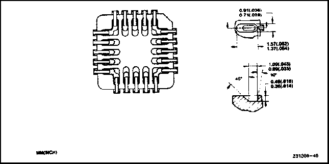
Figure 4B. Standard Package Bottom View (Tooling Option II.)
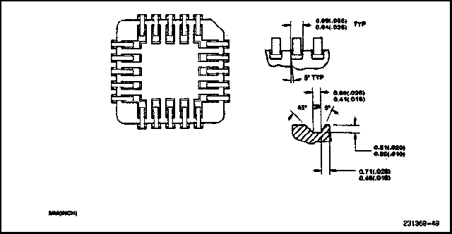
Figure 5. Detail J. Terminal Detail
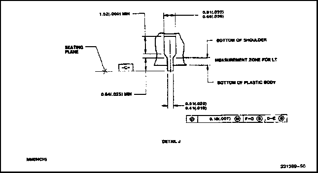
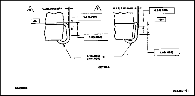
Figure 6. Detail L. Terminal Details.
Notes Square Package:
1. All dimensions nad tolerances conform to ANSI Y 14.5M-1982
2. Datum plane -H- located on top of mold parting line and coincidnet with top of lead, where lead exits plastic body.
3. Datums D-E and F-G to be determined wehre cente leads exit plasatic body at datum plane -H-.
4. To be determined at seating plane -C-
5. Dimension D1 and E1 do not include mold protrusion
6. Pin 1 identifier is located within one of the two defined zones.
7. Locations to datum -A- and -B- to be determined at plane -H-
8. These two dimensions determine maximum angle of the lead for certain socket applications. If unit is intenedt to be socketed, it is advisable to review these dimensions with the socket supplier.
9. Controlling dimension, inch.
10. All dimensions and tolerances include lead trim offset and lead plating finish.
11. Tweezing surface planarity is defined as the furtheset any lead on a side may be form the datum. The datum is established by touching the outermost lead on that side and parallel to D-E or F-G.
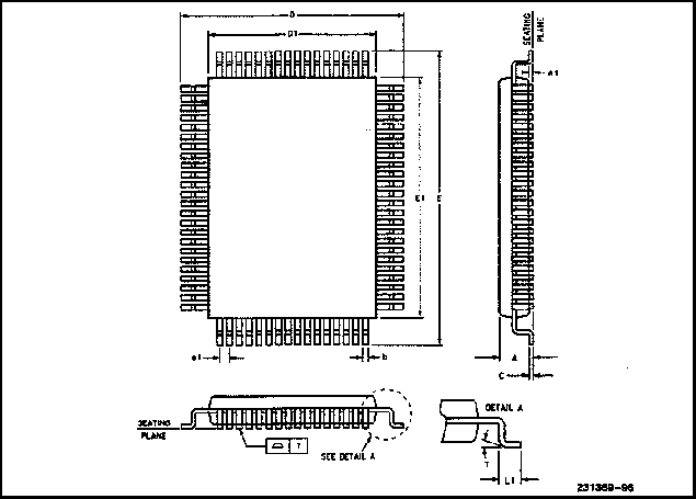
Quad Flatpack Package
Symbol list for Quad Flatpack Family
Letter or
Symbol | Description of Dimensions |
| N | Lead Count |
| A | Overall Height |
| A1 | Stand Off |
| AAA | Lead True Position |
| B | Lead Width |
| C | Lead Thickness |
| D | Terminal Dimension |
| D1 | Body Package |
| E | Terminal Dimension |
| E1 | Body Package |
| e1 | Lead Pitch |
| L1 | Foot Lenght |
| T | Lead Angle |
| Y | Coplanarity |
Note:
4. Not all packages are available with all products. Contact local FSE for further package information.
| Packaging Family Attributes |
| Category | Quad Flatpack |
| Acronym | QFE, SQFP, TQFP |
| Lead Configuration | Quad |
| Lead Counts | QFP 44, 64, 80, 100, 128, 160 - SQFP 80, 100, 208 - TQFP 144, 176 |
| Lead Finish | SolderPlate |
| Lead Pitch | 0.5, 0.65, 0.8 mm |
| Board Assembly Type | Socket and Surface Mount |
Note:
1. QFP- Alloy 42/copper on some lead frames. SWFP/TQFP copper lead frames only.
2. Novalac body.
3. Not all packages are availabel with all products. Contact local FSE for further package information.
| Shrink Quad Flatpack |
| Symbol | Description | Min | Nom | Max | Min | Nom | Max | Min | Max |
| N | Lead Count | 80 | 100 | 208 |
| A | Overall Height | | | 1.66 | | | 1.66 | 3.25 | 3.75 |
| A1 | Stand Off | 0.00 | | | 0.00 | | | 0 | 0.30 |
| b | Lead Width | 0.14 | 0.20 | 0.26 | 0.14 | 0.20 | 0.26 | 0.14 | 0.26 |
| c | Lead Thickness | 0.117 | 0.127 | 0.177 | 0.117 | 0.127 | 0.177 | 0.150 | 0.188 |
| D | Terminal Dimension | 13.70 | 14.00 | 14.30 | 15.70 | 16.0 | 16.30 | 30.2 | 31.0 |
| D1 | Package Body | | 12.0 | | | 14.0 | | 27.9 | 28.1 |
| E | Terminal Dimension | 13.70 | 14.00 | 14.30 | 15.70 | 16.0 | 16.30 | 30.2 | 31.0 |
| E1 | Package Body | | 12.0 | | | 14.0 | | 27.9 | 28.1 |
| e1 | Lead Pitch | 0.40 | 0.50 | 0.60 | 0.40 | 0.50 | 0.60 | 0.40 | 0.60 |
| L1 | Foot Length | 0.35 | 0.50 | 0.70 | 0.30 | 0.50 | 0.70 | 0.30 | 0.70 |
| T | Lead Angle | 0.0" | | 10.0* | 0.0* | | 10.0* | 0.0* | 10.0* |
| Y | Coplanarity | | | 0.10 | | | 0.10 | 0.1 |
| Thin Quad Flatpack |
| Symbol | Description
| Min | Max | Min | Max
|
| N | Lead Count | 144 | 176 |
| A | Overall Height | 1.3 | 1.7 | 1.3 | 1.7 |
| A1 | Stand Off | 0 | 0.20 | 0 | 0.20 |
| b | Lead Width | 0.16 | 0.28 | 0.16 | 0.28 |
| c | Lead Thickness | 0.122 | 0.160 | 0.122 | 0.160 |
| D | Terminal Dimension | 21.6 | 22.4 | 25.6 | 26.4 |
| D1 | Package Body | 19.9 | 20.1 | 23.9 | 24.1 |
| E | Terminal Dimension | 21.6 | 22.4 | 25.6 | 26.4 |
| E1 | Package Body | 19.9 | 20.1 | 23.9 | 24.1 |
| e1 | Lead Pitch | 0.40 | 0.60 | 0.40 | 0.60 |
| L1 | Foot Length | 0.40 | 0.80 | 0.40 | 0.80 |
| T | Lead Angle | 0.0* | 10.0* | 0.0* | 10.0* |
| Y | Coplanarity | 0.1 | 0.1 |
Note:
1. * Dimensions are in millimeters.
Figure 3. Principle dimensions and Data for QFP (Rectangular) Packages
| Quad Flatpack (Rectangular Packages) |
| Symbol | Description | Min | Nom | Max | Min | Nom | Max |
| N | Lead Count | 80 | 100 |
| A | Overall Height | | | 3.15 | | | 3.15 |
| A1 | Stand Off | 0.00 | | | 0.00 | | |
| b | Lead Width | 0.25 | 0.35 | 0.45 | 0.20 | 0.30 | 0.40 |
| c | Lead Thickness | 0.10 | 0.15 | 0.20 | 0.10 | 0.15 | 0.20 |
| D | Terminal Dimension | 17.5 | 17.9 | 18.3 | 17.5 | 17.9 | 18.3 |
| D1 | Package Body | | 14.0 | | | 14.0 | |
| E | Terminal Dimension | 23.5 | 23.9 | 24.3 | 23.5 | 23.9 | 24.3 |
| E1 | Package Body | | 20.0 | | | 20.0 | |
| e1 | Lead Pitch | 0.65 | 0.80 | 0.95 | 0.53 | 0.65 | 0.77 |
| L1 | Foot Length | 0.60 | 0.80 | 1.00 | 0.60 | 0.80 | 1.00 |
| T | Lead Angle | 0.0* | | 10.0* | 0.0* | | 10.0* |
| Y | Coplanarity | | | 0.10 | | | 0.10 |
Legal Stuff © 1997 Intel Corporation
