| AD0 | 17 | ALE/QS0 | 61 | RES | 24 | UCS | 34 | VCC | 9 |
| AD1 | 15 | BHE (RFSH) | 64 | RESET | 57 | LCS | 33 | VCC | 43 |
| AD2 | 13 | S0 | 52 | X1 | 59 | MCS0/PEREQ | 38 | VSS | 26 |
| AD3 | 11 | S1 | 53 | X2 | 58 | MCS1/ERROR | 37 | VSS | 60 |
| AD4 | 8 | S2 | 54 | CLKOUT | 56 | MCS2 | 36 | ||
| AD5 | 6 | RD/QSMD | 62 | TEST/BUSY | 47 | MCS3/NPS | 35 | ||
| AD6 | 4 | WR/QS1 | 63 | NMI | 46 | PCS0 | 25 | ||
| AD7 | 2 | ARDY | 55 | INT0 | 45 | PCS1 | 27 | ||
| AD8 (A8) | 16 | SRDY | 49 | INT1/SELECT | 44 | PCS2 | 28 | ||
| AD9 (A9) | 14 | DEN | 39 | INT2/INTA0 | 42 | PCS3 | 29 | ||
| AD10 (A10) | 12 | DT/R | 40 | INT3/INTA1 | 41 | PCS4 | 30 | ||
| AD11 (A11) | 10 | LOCK | 48 | PCS5/A1 | 31 | ||||
| AD12 (A12) | 7 | HOLD | 50 | PCS6/A2 | 32 | ||||
| AD13 (A13) | 5 | HLDA | 51 | TMR IN 0 | 20 | ||||
| AD14 (A14) | 3 | TMR IN 1 | 21 | ||||||
| AD15 (A15) | 1 | TMR OUT 0 | 22 | ||||||
| A16/S3 | 68 | TMR OUT 1 | 23 | ||||||
| A17/S4 | 67 | DRQ0 | 18 | ||||||
| A18/S5 | 66 | DRQ1 | 19 | ||||||
| A19/S6 | 65 | ||||||||
NOTE: Pin names in parantheses apply to the 80C188XL.
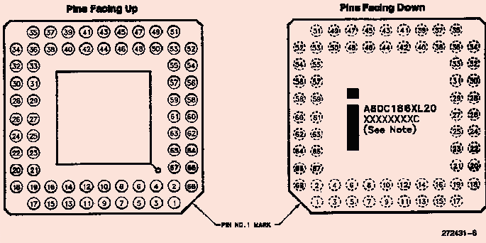
| 1 | AD15 (A15) | 18 | DRQ0 | 35 | MCS3/NPS | 52 | S0 |
| 2 | AD7 | 19 | DRQ1 | 36 | MCS2 | 53 | S1 |
| 3 | AD14 (A14) | 20 | TMR IN 0 | 37 | MCS1/ERROR | 54 | S2 |
| 4 | AD6 | 21 | TMR IN 1 | 38 | MCS0/PEREQ | 55 | ARDY |
| 5 | AD13 (A13) | 22 | TMR OUT 0 | 39 | DEN | 56 | CLKOUT |
| 6 | AD5 | 23 | TMR OUT 1 | 40 | DT/R | 57 | RESET |
| 7 | AD12 (A12) | 24 | RES | 41 | INT3/INTA1 | 58 | X2 |
| 8 | AD4 | 25 | PCS0 | 42 | INT2/INTA0 | 59 | X1 |
| 9 | VCC | 26 | VSS | 43 | VCC | 60 | VSS |
| 10 | AD11 (A11) | 27 | PCS1 | 44 | INT1/SELECT | 61 | ALE/QS0 |
| 11 | AD3 | 28 | PCS2 | 45 | INT0 | 62 | RD/QSMD |
| 12 | AD10 (A10) | 29 | PCS3 | 46 | NMI | 63 | WR/QS1 |
| 13 | AD2 | 30 | PCS4 | 47 | TEST/BUSY | 64 | BHE (RFSH) |
| 14 | AD9 (A9) | 31 | PCS5/A1 | 48 | LOCK | 65 | A19/S2 |
| 15 | AD1 | 32 | PCS6/A2 | 49 | SRDY | 66 | A18/S3 |
| 16 | AD8 (A8) | 33 | LCS | 50 | HOLD | 67 | A17/S4 |
| 17 | AD0 | 34 | UCS | 51 | HLDA | 68 | A16/S3 |
Note: Pin names in parentheses apply to the 80C188XL.
| AD0 | 64 | ALE/QS0 | 10 | RES | 55 | UCS | 45 | NC | 2 | VCC | 33 |
| AD1 | 66 | BHE (RFSH) | 7 | RESET | 18 | LCS | 46 | NC | 11 | VCC | 34 |
| AD2 | 68 | S0 | 23 | X1 | 16 | MCS0/PEREQ | 39 | NC | 14 | VCC | 72 |
| AD3 | 70 | S1 | 22 | X2 | 17 | MCS1/ERROR | 40 | NC | 15 | VCC | 73 |
| AD4 | 74 | S2 | 21 | CLKOUT | 19 | MCS2 | 41 | NC | 24 | VSS | 12 |
| AD5 | 76 | RD/QSMD | 9 | TEST/BUSY | 29 | PCS3/NPS | 42 | NC | 43 | VSS | 13 |
| AD6 | 78 | WR/QS1 | 8 | NMI | 30 | PCS0 | 54 | NC | 44 | VSS | 53 |
| AD7 | 80 | ARDY | 20 | INT0 | 31 | PCS1 | 52 | NC | 62 | ||
| AD8 (A8) | 69 | SRDY | 27 | INT1/SELECT | 32 | PCS2 | 51 | NC | 63 | ||
| AD9 (A9) | 67 | DEN | 38 | INT2/INTA | 36 | PCS3 | 50 | ||||
| AD10 (A 10) | 69 | DT/R | 37 | INT3/INTA1 | 36 | PCS4 | 49 | ||||
| AD11 (A11) | 71 | LOCK | 28 | PCS5/A1 | 48 | ||||||
| AD12 (A12) | 75 | HOLD | 26 | PCS6/A2 | 47 | ||||||
| AD13 (A13) | 77 | HLDA | 25 | TMR IN 0 | 59 | ||||||
| AD14 (A14) | 79 | TMR IN 1 | 58 | ||||||||
| AD15 (A15) | 1 | TMR OUT 0 | 59 | ||||||||
| A16/S3 | 3 | TMR OUT 1 | 56 | ||||||||
| A17/S4 | 4 | DRQ0 | 61 | ||||||||
| A18/S5 | 5 | DRQ1 | 60 | ||||||||
| A19/S6 | 6 | ||||||||||
Note: Pin names in parantheses apply to the 80C188XL.
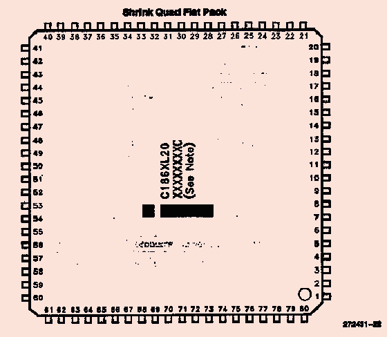
| 1 | AD15 (A15) | 21 | S2 | 41 | MCS2 | 61 | DRQ0 |
| 2 | NC | 22 | S1 | 42 | MCS3/NPS | 62 | NC |
| 3 | A16/S3 | 23 | S0 | 43 | NC | 63 | NC |
| 4 | A17/S4 | 24 | NC | 44 | NC | 64 | AD0 |
| 5 | A18/S5 | 25 | HLDA | 45 | UCS | 65 | AD8 (A8) |
| 6 | A19/S6 | 26 | HOLD | 46 | LCS | 66 | AD1 |
| 7 | BHE/(RFSH) | 27 | SRDY | 47 | PCS6/A2 | 67 | AD9 (A9) |
| 8 | WR/QS1 | 28 | LOCK | 48 | PCS5/A1 | 68 | AD2 |
| 9 | RD/QSMD | 29 | TEST/BUSY | 49 | PCS4 | 69 | AD10 (A10) |
| 10 | ALE/QS0 | 30 | NMI | 50 | PCS3 | 70 | AD3 |
| 11 | NC | 31 | INT0 | 51 | PCS2 | 71 | AD11 (A11) |
| 12 | VCC | 32 | INT1/SELECT | 52 | PCS1 | 72 | VCC |
| 13 | VCC | 33 | VCC | 53 | VCC | 73 | VCC |
| 14 | NC | 34 | VCC | 54 | PCS0 | 74 | AD4 |
| 15 | NC | 35 | INT2/INTA0 | 55 | RES | 75 | AD12 (A12) |
| 16 | X1 | 36 | INT3/INTA1 | 56 | TMR OUT 1 | 76 | AD5 |
| 17 | X2 | 37 | DT/R | 57 | TMR OUT 0 | 77 | AD13 (A13) |
| 18 | RESET | 38 | DEN | 58 | TMR IN 1 | 78 | AD6 |
| 19 | CLKOUT | 39 | MCS0/PEREQ | 59 | TMR IN 0 | 79 | AD14 (A14) |
| 20 | ARDY | 40 | MCS1/ERROR | 60 | DRQ1 | 80 | AD7 |
Note: Pin names in parentheses apply to the 80C188XL.
| AD0 | 1 | ALE/QS0 | 29 | RES | 73 | UCS | 62 | NC | 4 | VCC | 10 |
| AD1 | 3 | BHE (RFSH) | 26 | RESET | 34 | LCS | 63 | NC | 25 | VCC | 11 |
| AD2 | 6 | S0 | 40 | X1 | 32 | MCS0/PEREQ | 57 | NC | 35 | VCC | 20 |
| AD3 | 8 | S1 | 39 | X2 | 33 | MCS1/ERROR | 58 | NC | 55 | VCC | 550 |
| AD4 | 12 | S2 | 38 | CLKOUT | 36 | MCS2 | 59 | NC | 72 | VCC | 51 |
| AD5 | 14 | RD/QSMD | 28 | TEST/BUSY | 46 | MCS3/NPS | 60 | VCC | 61 | ||
| AD6 | 16 | WR/QS1 | 27 | NMI | 47 | PCS0 | 71 | VSS | 30 | ||
| AD7 | 18 | ARDY | 37 | INT0 | 48 | PCS1 | 69 | VSS | 31 | ||
| AD8 (A8) | 2 | SRDY | 44 | INT1/SELECT | 49 | PCS2 | 68 | VSS | 41 | ||
| AD9 (A9) | 5 | DEN | 56 | INT2/INTA0 | 52 | PCS3 | 67 | VSS | 70 | ||
| AD10 (A10) | 7 | DT/R | 54 | INT3/INTA1 | 53 | PCS4 | 66 | VSS | 80 | ||
| AD11 (A11) | 9 | LOCK | 45 | PCS5/A1 | 65 | ||||||
| AD12 (A12) | 13 | HOLD | 43 | PCS6/A2 | 64 | ||||||
| AD13 (A13) | 15 | HLDA | 43 | TMR IN 0 | 77 | ||||||
| AD14 (A14) | 17 | TMR IN 1 | 76 | ||||||||
| AD15 (A15) | 19 | TMR OUT 0 | 75 | ||||||||
| A16/S3 | 21 | TMR OUT 1 | 74 | ||||||||
| A17/S4 | 22 | DRQ0 | 79 | ||||||||
| A18/S5 | 23 | DRQ1 | 78 | ||||||||
| A19/S6 | 24 | ||||||||||
Note: Pin names in parentheses apply to the 80C188XL.
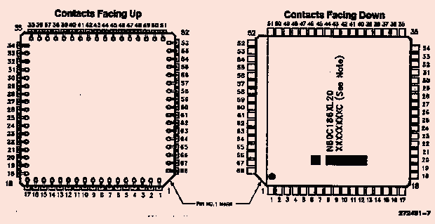
| 1 | AD0 | 21 | A16/S3 | 41 | VSS | 61 | VCC |
| 2 | AD8 (A8) | 22 | A17/S4 | 42 | HLDA | 62 | UCS |
| 3 | AD1 | 23 | A18/S5 | 43 | HOLD | 63 | LCS |
| 4 | NC | 24 | A19/S6 | 44 | SRDY | 64 | PCS6/A2 |
| 5 | AD9 (A9) | 25 | NC | 45 | LOCK | 65 | PCS5/A1 |
| 6 | AD2 | 26 | BHE (RFSH) | 46 | TEST/BUSY | 66 | PCS4 |
| 7 | AD10 (A10) | 27 | WR/QS1 | 47 | NMI | 67 | PCS3 |
| 8 | AD3 | 28 | RD/QSMD | 48 | INT0 | 68 | PCS2 |
| 9 | AD11 (A11) | 29 | ALE/QS0 | 49 | INT1/SELECT | 69 | PCS1 |
| 10 | VCC | 30 | VSS | 50 | VCC | 70 | VSS |
| 11 | VCC | 31 | VSS | 51 | VCC | 71 | PCS0 |
| 12 | AD4 | 32 | X1 | 52 | INT2/INTA0 | 72 | NC |
| 13 | AD12 (A12) | 33 | X2 | 53 | INT3/INTA1 | 73 | RES |
| 14 | AD5 | 34 | RESET | 54 | DT/R | 74 | TMR OUT 1 |
| 15 | AD13 (A13) | 35 | NC | 55 | NC | 75 | TMR OUT 0 |
| 16 | AD6 | 36 | CLKOUT | 56 | DEN | 76 | TMR IN 1 |
| 17 | AD14 (A14) | 37 | ARDY | 57 | MCS0/PEREQ | 77 | TMR IN 0 |
| 18 | AD7 | 38 | S2 | 58 | MCS1/ERROR | 78 | DRQ1 |
| 19 | AD15 (A15) | 39 | S1 | 59 | MCS2 | 79 | DRQ0 |
| 20 | VCC | 40 | S0 | 60 | MCS3/NPS | 80 | VSS |
Note: Pin names in parentheses apply to the 80C188XL.
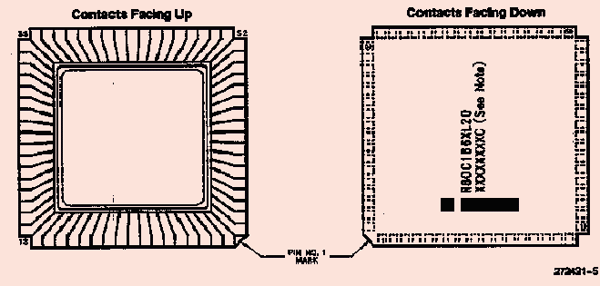
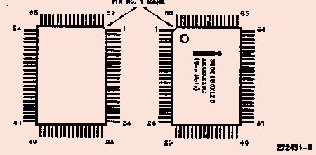
Figure 4. 80C186XL/80CL188XL Pinout Diagrams
Ceramic Pin Grid Array
Note: XXXXXXXXC indicates the Intel FPO number.
Note: XXXXXXXXC indicates the Intel FPO number.
80-Pin Quad Flat Pack (EIAJ)
Note: XXXXXXXXA indicates the Intel FPO number.
Plastic Leaded Chip Carrier Package
Symbol List for Plastic Leaded Chip Carrier Family
| A | Overall Height: Distance from seating plane to highest point of body |
| A1 | Distance from lead shoulder to seating plane |
| CP | Seating plane coplanarity |
| D/E | Overall package dimension |
| D1/E1 | Plastic body dimension |
| D2/E2 | Footprint |
| LT | Lead thickness |
| N | Total number of leads |
| Nd | Total number of leads on short side |
| Ne | Total number of leads on long side |
| TCP | Tweezing coplanarity |
Notes: Rectangle Package
| Packaging Family Attributes | |
| Category | Plastic Leaded Chip Carrier |
| Acronym | PLCC |
| Lead Configuration | Quad |
| Lead Counts | 28, 32, 44, 52, 68, 84 |
| Lead Finish | SolderPlate |
| Lead Pitch | 0.50" |
| Board Assembly Type | Socket and Surface Mount |
Notes:
| Family: Plastic Leaded Chip Carrier-Square (mm) | |||||||||
| A | 0.165 | 0.180 | 4.19 | 4.83 | 4.19 | 4.83 | |||
| A1 | 0.090 | 0.120 | 2.29 | 3.05 | 2.29 | 3.05 | |||
| D | 0.785 | 0.795 | 25.0 | 25.3 | 30.1 | 30.4 | |||
| D1 | 0.750 | .0756 | 24.1 | 24.3 | 29.2 | 29.4 | |||
| D2 | 0.690 | 0.730 | 22.6 | 23.6 | 27.7 | 28.7 | |||
| E | 0.785 | 0.795 | 25.0 | 25.3 | 30.1 | 30.4 | |||
| E1 | 0.750 | 0.756 | 24.1 | 24.3 | 29.2 | 29.4 | |||
| E2 | 0.690 | 0.730 | 22.6 | 23.6 | 27.7 | 28.7 | |||
| N | |||||||||
| CP | 0.000 | 0.004 | 0.00 | 0.10 | 0.00 | 0.10 | |||
| TCP | 0.000 | 0.004 | 0.00 | 0.10 | 0.00 | 0.10 | |||
| LT | 0.009 | 0.015 | 0.20 | 0.36 | 0.20 | 0.36 | |||
| Family: Plastic Leaded Chip Carrier-Square (inch) | |||||||||
| 84 Lead | |||||||||
| A | 01.65 | 0.180 | 0.165 | 0.190 | 0.165 | 0.190 | |||
| A1 | 0.090 | 0.120 | 0.090 | 0.120 | 0.090 | 0.120 | |||
| D | 0.785 | 0.795 | 0.985 | 0.995 | 1.185 | 1.195 | |||
| D1 | 0.750 | 0.756 | 0.950 | 0.958 | 1.150 | 1.158 | |||
| D2 | 0.690 | 0.730 | 0.890 | 0.930 | 1.090 | 1.130 | |||
| E | 0.785 | 0.795 | 0.985 | 0.995 | 1.185 | 1.195 | |||
| E1 | 0.750 | 0.756 | 0.950 | 0.958 | 1.150 | 1.158 | |||
| E2 | 0.690 | 0.730 | 0.890 | 0.930 | 1.090 | 1.130 | |||
| N | |||||||||
| CP | 0.000 | 0.004 | 0.000 | 0.004 | 0.000 | 0.004 | |||
| TCP | 0.000 | 0.004 | 0.000 | 0.004 | 0.000 | 0.004 | |||
| LT | 0.009 | 0.015 | 0.008 | 0.014 | 0.008 | 0.014 | |||
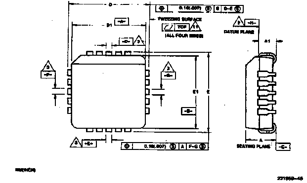
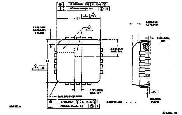
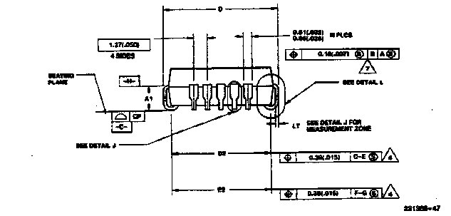
Figure 3. Terminal Details
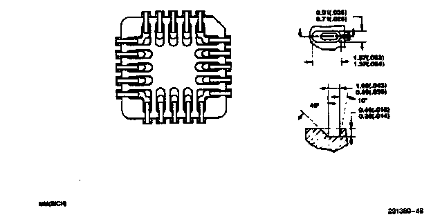
Figure 4A. Standard Package Bottom View (Tooling Option I.)
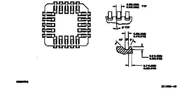
Figure 4B. Standard Package Bottom View (Tooling Option II.)
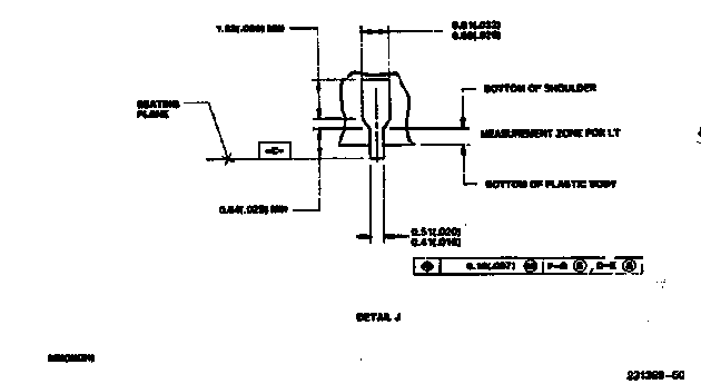
Figure 5. Detail J. Terminal Detail
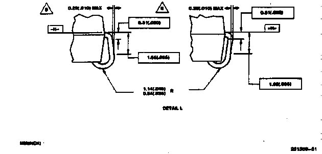
Figure 6. Detail L. Terminal Details
Notes Square Package:
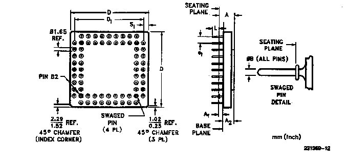
Symbol List for Ceramic Pin Grid Array Family
| A | Distance from seating plane to highest point of body |
| A1 | Distance between seating plane and base plane |
| A2 | Distance from base plane to highest point of body |
| A3 | Distance from seating plane to bottom of body |
| A4 | Heat spreader thickness |
| B | Diameter of terminal lead pin |
| D | Largest overall package dimension of length |
| D1 | A body length dimension, outer lead center to outer lead center |
| D2 | Head spreader length and width |
| e1 | Linear spacing between true lead position centerlines |
| L | Distance from seating plane to end of lead |
| S1 | Other body dimension, outer lead center to edge of body |
Notes:
| Packaging Family Attributes | |
| Category | Ceramic Pin Grid Array |
| Acronym | C-PGA or PGA |
| Lead Configuration | Array |
| Lead Counts | 68, 88, 132, 168-208, 240-280, 272-320 |
| Lead Finish | Gold Plate, 60 Microinches of Gold over 100-350 Microinches of Nickel Plate |
| Lead Material | Kovar or Alloy 42 |
| Lead Braze Material | Copper/Silver Eutectic |
| Lead Pitch | 0.100" |
| Board Assembly Type | Socket and Insertion Mount |
Notes:
| Symbol | ||||||
| A | 4.06 | 5.21 | EPROM Lid | 0.160 | 0.205 | EPROM Lid |
| A | 3.30 | 4.32 | Solid Lid | 0.130 | 0.170 | Solid Lid |
| A1 | 1.14 | 1.40 | 0.045 | 0.055 | ||
| A2 | 2.16 | 3.18 | Solid Lid | 0.085 | 0.125 | Solid Lid |
| A2 | 2.67 | 3.94 | EPROM Lid | 0.105 | 0.155 | EPROM Lid |
| B | 0.43 | 0.51 | 0.017 | 0.020 | ||
| D | 28.96 | 29.97 | 1.140 | 1.180 | ||
| D1 | 25.27 | 25.53 | 0.995 | 1.005 | ||
| e1 | 2.29 | 2.79 | 0.090 | 0.110 | ||
| L | 2.54 | 3.30 | 0.100 | 0.130 | ||
| N | ||||||
| S1 | 1.27 | 2.54 | 0.050 | 0.100 | ||
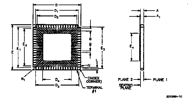
Ceramic Leadless Chip Carrier
Symbol List for Ceramic Leadless Chip Carrier Family
| A | Thickness of base body |
| A1 | Total package height |
| A2 | Distance from base body to highest point of body (lid) |
| B | Width of terminal lead pin |
| D | Largest overall package dimension of length |
| D1,E1 | A body length dimension, corner cutout to corner cutout or end lead center to end lead center |
| D2,E2 | A body length dimension, end lead center to end lead center |
| D3,E3 | A body length dimension, corner cutout to index corner cutout |
| D4,E4 | Ceramic body fixture |
| E | Largest overall package dimension of width |
| e | Linear spacing |
| e1 | Linear spacing between edges of tur elead positions (of corner terminal lead pads) lead corner to lead corner |
| h | Depth of major index feature |
| j | Width of minor index feature |
| L | Distance from package edge to end of effective pad |
| N | The total number of potentially useable lead positions |
| R1 | Inner notch radius |
Notes:
| Packaging Family Attributes | |
| Category | Ceramic Leadless Chip Carrier |
| Acronym | LCC |
| Lead Configuration | N/A |
| Lead Counts | 18, 20, 28, 32, 44, 68 |
| Lead Finish | Gold Plate |
| Lead Pitch | 0.050" |
| Board Assembly Type | Socket and Surface Mount |
Notes:
68 Ceramic Leadless Chip Carrier Variation: Die Down
| A | 1.37 | 1.68 | 0.054 | 0.066 | ||
| A1 | 2.16 | 2.72 | 0.085 | 0.107 | ||
| B | 0.84 | 0.99 | Typical | 0.033 | 0.039 | Typical |
| D | 23.88 | 24.38 | 0.940 | 0.960 | ||
| D1 | 21.39 | 21.39 | 0.842 | 0.858 | ||
| D2 | Reference | Reference | ||||
| D3 | Reference | Reference | ||||
| D4 | 16.76 | 17.27 | 0.660 | 0.680 | ||
| E | 23.88 | 24.38 | 0.940 | 0.960 | ||
| E1 | 21.39 | 21.79 | 0.842 | 0.858 | ||
| E2 | Reference | Reference | ||||
| E3 | Reference | Reference | ||||
| E4 | 16.76 | 17.27 | 0.660 | 0.680 | ||
| e | 1.04 | 1.50 | Typical | 0.041 | 0.059 | Typical |
| L | 0.94 | 0.037 | ||||
| N | ||||||
| R1 | 0.25 | 0.010 | ||||
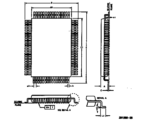
Symbol List for Quad Flatpack Family
| N | Lead Count |
| A | Overall Height |
| A1 | Stand Off |
| AAA | Lead True Position |
| B | Lead Width |
| C | Lead Thickness |
| D | Terminal Dimension |
| D1 | Body Package |
| E | Terminal Dimension |
| E1 | Body Package |
| e1 | Lead Pitch |
| L1 | Foot Length |
| T | Lead Angle |
| Y | Coplanarity |
Note: Not all packages are available with all products. Contact local FSE for further package information.
| Packaging Family Attributes | |
| Category | Quad Flatpack |
| Acronym | QFP, SQFP, TQFP |
| Lead Configuration | Quad |
| Lead Counts | QFP 44, 48; 64, 80, 100, 128, 160 - SQFP 80, 100; 208 - TQFP 144, 176 |
| Lead Finish | SolderPlate |
| Lead Pitch | 0.5, 0.65, 0.8 mm |
| Board Assembly Type | Socket and Surface Mount |
Note:
| Symbol | Description | Min | Nom | Max | Min | Nom | Max | Min | Max |
| N | Lead Count | ||||||||
| A | Overall Height | 1.66 | 1.66 | 3.25 | 3.75 | ||||
| A1 | Stand Off | 0.00 | 0.00 | 0 | 0.30 | ||||
| b | Lead Width | 0.14 | 0.20 | 0.26 | 0.14 | 0.20 | 0.26 | 0.14 | 0.26 |
| c | Lead Thickness | 0.117 | 0.127 | 0.177 | 0.117 | 0.127 | 0.177 | 0.150 | 0.188 |
| D | Terminal Dimension | 13.70 | 14.00 | 14.30 | 15.70 | 16.0 | 16.30 | 30.2 | 31.0 |
| D1 | Package Body | 12.0 | 14.0 | 27.9 | 28.1 | ||||
| E | Terminal Dimension | 13.70 | 14.0 | 14.30 | 15.70 | 16.00 | 16.30 | 30.2 | 31.0 |
| E1 | Package Body | 12.0 | 14.0 | 27.9 | 28.1 | ||||
| e1 | Lead Pitch | 0.40 | 0.50 | 0.60 | 0.40 | 0.50 | 0.60 | 0.40 | 0.60 |
| L1 | Foot Length | 0.35 | 0.50 | 0.70 | 0.30 | 0.50 | 0.70 | 0.30 | 0.70 |
| T | Lead Angle | 0.0" | 10.0" | 0.0" | 10.0" | 0.0" | 10.0" | ||
| Y | Coplanarity | 0.10 | 0.10 | ||||||
| Symbol | Description | Min | Max | Min | Max |
| N | Lead Count | ||||
| A | Overall Height | 1.3 | 1.7 | 1.3 | 1.7 |
| A1 | Stand Off | 0 | 0.20 | 0 | 0.20 |
| b | Lead Width | 0.16 | 0.28 | 0.16 | 0.28 |
| c | Lead Thickness | 0.122 | 0.160 | 0.122 | 0.160 |
| D | Terminal Dimension | 21.6 | 22.4 | 25.6 | 26.4 |
| D1 | Package Body | 19.9 | 20.1 | 23.9 | 24.1 |
| E | Terminal Dimension | 21.6 | 22.4 | 25.6 | 26.4 |
| E1 | Package Body | 19.9 | 20.1 | 23.9 | 24.1 |
| e1 | Lead Pitch | 0.40 | 0.60 | 0.40 | 0.60 |
| L1 | Foot Length | 0.40 | 0.80 | 0.40 | 0.80 |
| T | Lead Angle | 0.0" | 10.0" | 0.0" | 10.0" |
| Y | Coplanarity | ||||
Note:
| Symbol | Description | Min | Nom | Max | Min | Nom | Max |
| N | Lead Count | ||||||
| A | Overall Height | 3.15 | 3.15 | ||||
| A1 | Stand Off | 0.00 | 0.00 | ||||
| b | Lead Width | 0.25 | 0.35 | 0.45 | 0.20 | 0.30 | 0.40 |
| c | Lead Thickness | 0.10 | 0.15 | 0.20 | 0.10 | 0.15 | 0.20 |
| D | Terminal Dimension | 17.5 | 17.9 | 18.3 | 17.5 | 17.9 | 18.3 |
| D1 | Package Body | 14.0 | 14.0 | ||||
| E | Teminal Dimension | 23.5 | 23.9 | 24.3 | 23.5 | 23.9 | 24.3 |
| E1 | Package Body | 20.0 | 20.0 | ||||
| e1 | Lead Pitch | 0.65 | 0.80 | 0.95 | 0.53 | 0.65 | 0.77 |
| L1 | Foot Length | 0.60 | 0.80 | 1.00 | 0.60 | 0.80 | 1.00 |
| T | Lead Angle | 0.0" | 10.0" | 0.0" | 10.0" | ||
| Y | Coplanarity | 0.10 | 0.10 | ||||
Legal Stuff © 1997 Intel Corporation
