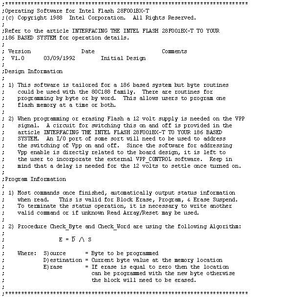
Why Should You Use FLASH?
FLASH provides an easy and cost effective method of implementing system firmware and configuration. It allowsremote, non hardware based upgrades. Flash can be erased electrically, unlike EPROMs and are typically higher density and cheaper than EEPROMs. Unlike battery backed RAM, Flash is nonvolatile. They are ideal for a Solid State disk/card, possibly storing data, an operating system, or even user information.
Flash Concerns
The 28F001BX-T provides 128K Bytes (1MBit) of CMOS Flash memory and contains many features, such as:
| Memory Blocks | Memory Address |
| One 8 Kb Boot Block w/lock out | 1E000 to 1FFFF |
| Two 4KB Parameter Blocks | 1D000 to 1DFFF 1C000 to 1CFFF |
| One 112KB Main Block |
To accommodate the 16 bit data bus of the C186, two Flash memories are used. Figure 1 illustrates the Flash interface to the 80C186. The chip enables are tied to UCS, which is configured for a 256K byte block size, starting at C0000H. This puts the Boot Block at FC000H. The Block Protect in Figure 1 will tie the PWD pin to VCC or +12VDC. If tied to VCC, it will not be possible to write to the Boot block, otherwise strapping it to 12 volts will allow erasure of the block. The signal VPPEN is used to turn on and off 12 volts to VPP. This line can be connected to one of the ports on the C186. When activating this signal, be sure to allow some switching time for the Mosfet transistor. The 12 volt supply should be stable and able to supply at least 60mA of current. The address lines (LA1-LA17) connected to the Flash need to be latched using ALE from the 80C186.
Program/Erasure
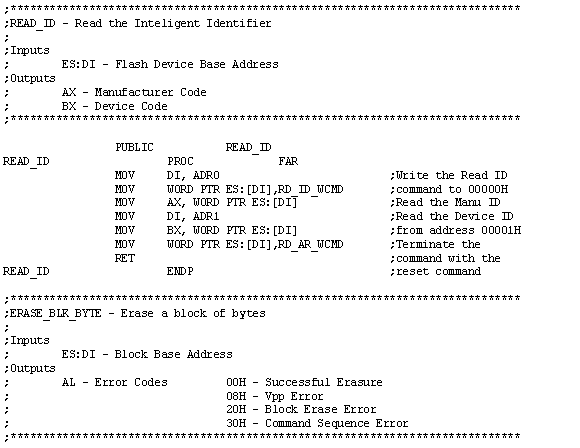
There are two registers provided on the 28F001BX Flash, one to write commands and the other to read the status of the device. The command register does not occupy any memory locations but instead is accessed during a write operation to the device. When using commands that are block specific it is necessary to write the command to an address within the block. Be sure to access the correct even or odd block address when doing byte operations.
Programming the Flash requires VPP to be driven to 12VDC. This can be accomplished by using a jumper to supply 12 volts to VPP or a port can be used. A circuit is provided for turning the 12 volts on or off using the VPPEN signal in Figure 1. The VPPEN signal should be controlled by an output port from the C186.
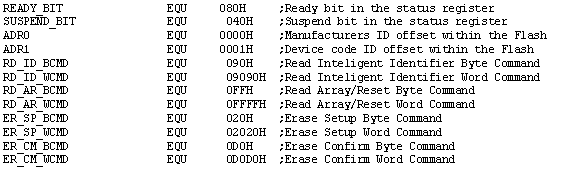
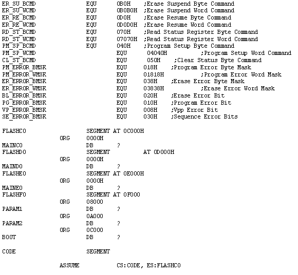
Commands
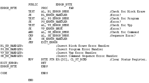
Definition of the Status Register:
Bit 3 VPP status
1= VPP is low and the operation was aborted. This bit must be
cleared before programming/erasing can be reattempted.
0= VPP is valid.
Bit 4 Program status
1= Error during byte programming.
0= Successful byte program.
Bit 5 Erase status
1= Error in block erasure. When both Bit 5 and Bit 4 are set,
then an improper erase command sequence was entered.
0= Successful block erase.
Bit 6 Erase Suspend Status
1= Erase Suspended.
0= Erase in Progress/Completed.
Bit 7 Write State Machine Status
1= Ready.
0= Busy.
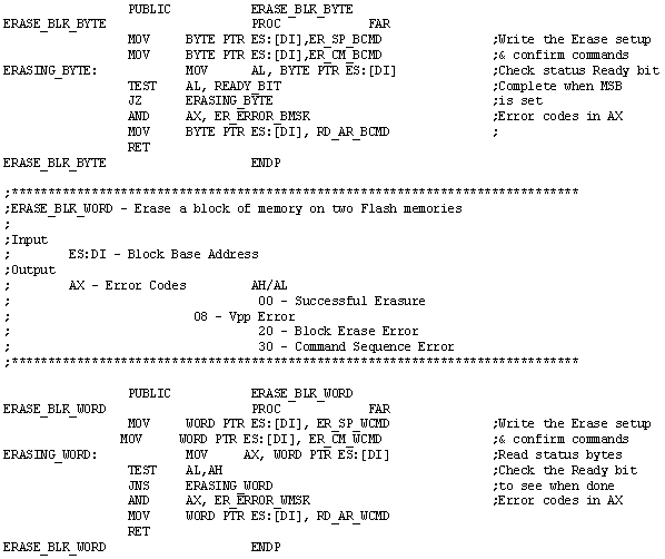
Block Erasure
To erase a block, first write the command 20H to an address in the block. Next confirm the erasure by writing D0H to the block. Because the command register does not occupy an addressable memory location, the only requirement is the written address be within the block. Once written, wait until the Write State Machine status bit is ready. If this wait is too long it may be necessary to suspend the erasure and check the status and memory. When the erasure is finished the Erase, Program, and VPP status bits need to be checked for errors. If no errors were detected then the block was successfully erased. The algorithm for erasing a block is summarized in Flowchart 1.
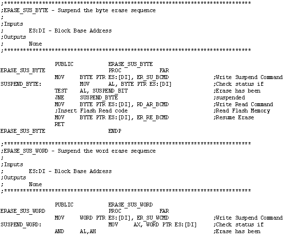
Suspend/Resume Block Erasure
To suspend block erasure, write the command B0H to the block address. Next, check the Erase Suspend Status bit until it is Ready or set. The status bit needs to be checked because the Flash will not suspend its erasure until it reaches a checkpoint in its program. The Read Array command (0FFH) is written to return the device into the read mode. It is then possible to read the memory. When finished reading the memory, writing the command (D0H) to any address within the block will resume the erasure.
The algorithm for suspending and resuming an erasure is summarized by Flowchart 2. If an error is detected by the status register, the status register must be cleared before attempting the erasure.
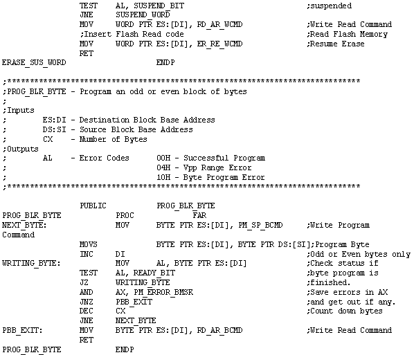
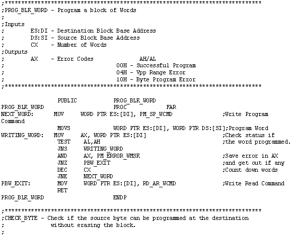
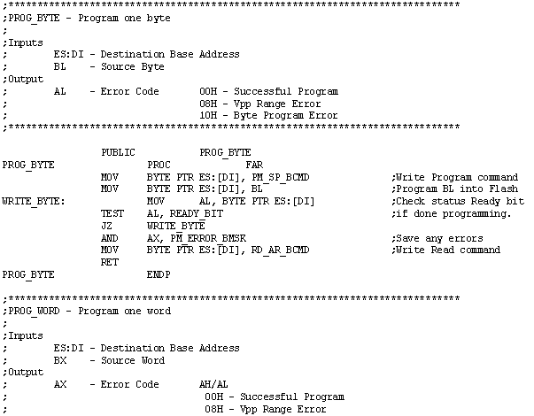
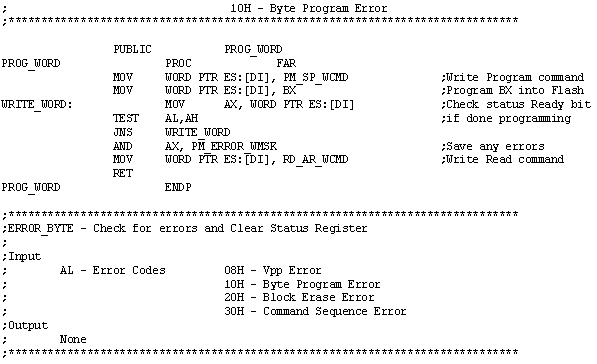
Byte Programming
Programming the Flash starts with writing the Program Setup command (040H) to the address of the byte to be programmed. Next, write the data to the same address. When done, check the Program and VPP status bits for errors. If no errors were detected then the byte was successfully programmed. The algorithm for programming a byte is summarized by Flowchart 3.
Programming Tips
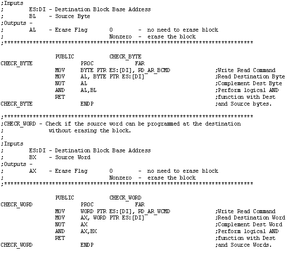
When programming Flash, the location to be programmed must be erased first. To erase the location the entire block will need to be erased. A byte is erased when all 8 bits are set (0FFH). But in reality it is possible to program a byte even if the bits are not all set. The program only needs to check that all of the source bits that are set are also set at the destination. This is useful if programming only a specific location and not a range of locations. This can be achieved by ANDing the Source with the compliment of the Destination:
_
E = D /\ S
Where: S)ource = Byte to be programmed
D)estination = Current byte value at the memory location
E)rase = If erase is equal to zero then the location can be programmed with the new byte otherwise the block will need to be erased.
It is also possible to program both the hi and low Flash devices at the same time. Commands need to be given in both the hi and low byte of the word. If there are interrupt service routines that may access the Flash memory then it is important to disable interrupts while programming or erasing the device. Thanks to Flash automation if the interrupt service routine does not access the Flash then there is no need to disable the interupt while programming/erasing.
Flash memory devices may program or erase at different rates. Therefore when programming or erasing both Flash devices simultaneously it is important to verify both.
Programming Routine
Source Code For Programming Routine

Legal Stuff © 1997 Intel Corporation
