Introduction
The 186 family of embedded processors are essentially an enhanced 8086 core with several common peripherals integrated on the same die. The enhanced core contains additional features that the original 8086 didn't have such as 7 additional instructions and a static core. The integrated peripherals include useful devices such as timer/counters, an interrupt control unit and a chip select unit, etc.
The 8086 core has two external interrupt sources; the Non-Maskable Interrupt (NMI) and a single maskable interrupt source. The NMI interrupt input of the core is brought directly out to the NMI pin of the 186. For most embedded designs, a single maskable interrupt input is not sufficient. In order to expand the capabilities of the single maskable interrupt an interrupt controller is needed.
Unlike other members of the 186 Family of Embedded Microprocessors, the 80C18xEC proliferation uses a 82C59A-2 compatible interrupt control unit instead of a proprietary-type controller. Located on the 80C18xEC die are two 82C59A-2 compatible Programmable Interrupt Controllers (PIC). One PIC is configured as the master while the other is configured as a slave. The slave is attached to the IR7 line of the master.
The 82C59A-2 has 8 configurable interrupt request lines and has the capability to cascade other 82C59A-2 PICs to give a total of 64 possible interrupt request lines. Each cascaded 82C59A-2 is called a slave; there can be only 1 master PIC. The master PIC of the 80C18xEC prioritizes interrupt requests from attached slaves and IR lines and presents requests, one at a time, to the single maskable interrupt line of the 808x core.
The 82C59A-2 is an industry standard interrupt controller for embedded solutions and also for the PC-compatible industry. Because of its wide use, it was decided that this PIC be an internal integrated peripheral of the 80C18xEC.
This document was not intended to be a stand alone document but should be used in conjunction with the 80C18xEC User's Manual and the 82C59A-2 Data Sheet found in the Peripheral Handbook (Intel Literature order numbers are 272047 and 296467 respectively).
Overview
The 186 Family of Embedded Processors can detect up to 256 different types of interrupts. Each interrupt is specified by its interrupt type ranging from 0 to 255. Each interrupt type has a corresponding interrupt vector which is the interrupt type multiplied by 4. A vector is a double word pointer that points to the associated Interrupt Service Routine (ISR). An interrupt vector table in memory stores up to 256 interrupt vectors. The first word of the vector contains the offset of the associated ISR while the second word contains the segment. This makes each vector a total of 4 bytes. The interrupt vector table is located at the base of the 186's memory map (0000:0000). The interrupt vector table is 1K byte in length (4 bytes multiplied by 256 types) and therefore goes up to (0000:03FF). Because of the location of the interrupt vectors, the lower 1K byte of memory space should be reserved for interrupt vectors.
Interrupt Processing
When an interrupt occurs, several steps are taken by the processor:
1.A partial machine status is saved/copied by pushing the Program Status Word (PSW) onto the stack
2. The Trap Flag (TF) bit and the Interrupt Enable (IE) bit are cleared in the PSW.
Upon completion of the ISR, the programmer must take several steps:
1. If the interrupt came from one of the request lines of the PIC (i.e. not a Divide by Zero interrupt) then the In-Service bit for that particular interrupt source must be cleared (discussed later on in this document).
When an IRET instruction is executed, the processor takes the following steps:
82C59 Programming
Initialization Command Words
The Initialization Command Words (ICWs) are programmed in a sequencial format and are used to set up the integrated interrupt controller to an initial state of operation. Typically, the ICW registers are programmed only once and are left untouched for the duration of the application. This section has been designed to highlight some of the subtleties associated with the functionality of each register and with accessing each register.
ICW1 Beginning of Initialization Register
ICW1 is used to select level or edge sensitive triggering on the IR lines, the number of 82C59's in the system and to indicate whether or not the ICW4 register will be used in the initialization sequence.
ICW1 Note:
Mixed triggering types is not possible. Either all of IR0 through IR7 is level sensitive or edge sensitive, but not both.
There are some subtle differences between edge and level sensitive interrupts. If an IR line is configured as level sensitive and is left asserted while it is serviced, the processor will imediately vector back into the ISR once the EOI is issued. Therefore, if configured as level sensitive, the IR line must be deasserted before issuing the EOI command inside the ISR. If the IR line is configured as edge sensitive, the processor will not vector back into the ISR if the IR line is kept asserted once the EOI has been issued. In order for another interrupt to occur on a edge sensitive IR line, the line must be brought to its inactive state for 100 ns to reset the edge detection circuitry.
ICW1 Access:
ICW1 is a write only register that is accessed through MPICP0 or SPICP0 with data bit position 4 set. See ICW Initialization Sequence.
ICW2 Base Interrupt Type Register
The data written to this register corresponds to the base interrupt type. The base interrupt type is synonomous with the interupt type for IR0. Once the base type has been defined each subsequent IRx line will have a TYPE = BASE + x. The interrupt vectors for each IR line will be at the location TYPE*4 in memory.
If an IR line is configured as a cascaded input, it will still have an associated type (interrupt vector), but in most cases, it will not be used. A case in which the interrupt vector would be used is if IR7 is configured as a cascaded input and is also used to detect spurious interrupts. In this case, if the processor vectors to the IR7 interrupt vector, the only reason it would do so is because a spurious interrupt was detected.
ICW2 Access:
ICW2 is a write only register which is accessed by a write to MPICP1 or SPICP1 immediately after ICW1 has been configured. See ICW Initialization Sequence.
ICW3 Cascaded Input Selection/Slave ID
ICW3 of the master is used to select whether or not a slave will be connected to the associated IR line.
ICW3 of a slave is used to set the associated slave ID. The slave ID should match the IR line number of the master that it is connected to.
ICW3 Note:
Special precautions must be taken when connecting a slave to IR0 of a master 8259A module. A slave programmed for an ID of zero will be active for both interrupts that it has requested, as well as for uncascaded master interrupts (uncascaded interrupts leave the CAS lines inactive low). If this situation occurs there will be contention on the data bus as both the master and the slave attempt to drive the interrupt type on the data bus. Never cascade a slave 8259A module to IR0 of a master module unless IR0 is the last available uncascaded input (i.e. the system is fully cascaded with eight slave 8259A modules).
ICW3 Access:
ICW3 is a write only register. If the SNGL bit of ICW1 was cleared during the intitialization sequence then ICW3 can be accessed by a write to MPCIP1 or SPCIP1 immediately after ICW2 has been initialized. See ICW Initialization Sequence.
ICW4 Special Fully Nested Mode/ Automatic End of Interrupt Mode Register
ICW4 is a write only register. Special Fully Nested (SFN) Mode and Automatic End of Interrupt (AEOI) Mode are selected using ICW4.
ICW4 Notes:
none
ICW4 Access:
ICW4 is accessed by a write to MPICP1 or SPICP1 provided that the IC4 bit was set in ICW1 during the initialization sequence. See ICW Initialization Sequence.
ICW Initialization Sequence
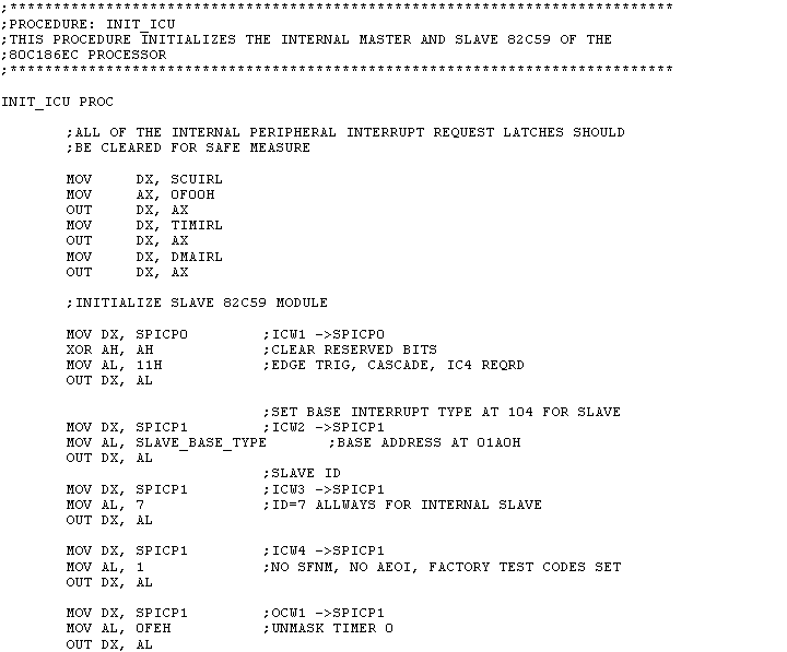
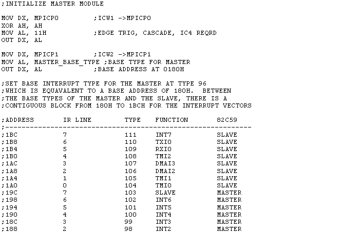
Before normal operation can begin, each 82C59 must be initialized by a sequence of two to four programming bytes called Initialization Command Words (ICWs). After reset, the states of all the 82C59 registers are undefined. The ICWs are used to set up the necessary conditions and modes for proper 82C59 operation. Minimum 82C59 initialization requires at least ICW1 and ICW2 to be configured. ICW3 and ICW4 are used only if designated in ICW1. The specific details of the function of each register is described in the 80C18xEC User's Manual. The sequence in which these registers is programmed is critical.
Note:
The ICW initialization sequence is started (or restarted) at ICW1 by writing data to MPICP0 or SPICP0 with the D4 bit set to a 1.
Figure 1 illustrates the initialization sequence of the ICW registers. Once the 82C59 is initialized, any changes to the ICWs are made by restarting the initialization sequence all over again from the beginning. In addition, should the initialization sequence be interrupted, the state machine can be reinitialized by re-starting the initialization process.
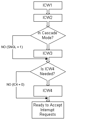
Once the initialization sequence has been started (ICW1 has been accessed), the 82C59 automatically performs the following events:
The complex initialization sequence exists because the original 8259 was designed with only one address line. Without the use of a initialization sequence (state machine), a device with only one address line would only have the potential of accessing only two registers (ports). By implementing an initialization sequence (state machine implementation), designers could keep the size of the chip down (using only one address line) and still access more than two registers.
In all, write accesses to the Initialization Command Words of the 82C59 are controlled by the following:
| Port Name | PCB Offset | A1 of Processor A0 of 82C59A-2 |
| MPICP0 | 00 | 0 |
| SPICP0 | 04 | 1 |
| MPICP1 | 02 | 0 |
| SPICP1 | 06 | 1 |
The first character of the port name indicates which internal 82C59 port is referenced: "M" indicates the Master PIC and "S" indicates the Slave.
Operational Command Words
Once the 82C59 has been initialized using the ICWs, the Operational Command Words (OCWs) can be used to modify priority schemes, End of Interrupt (EOI) configurations and interrupt masking.
Three OCWs are available for programming but, unlike the ICWs, accessing the OCW registers needn't be in any specific order. These registers can be accessed whenever the programmer desires, provided that the ICWs have been previously initialized. Although there is no accessing sequence to the OCWs, accessing each OCW and accompaning register (described later) is not intuitive. A detailed description of the OCW registers is given in the 80C18xEC User's Manual. This section has been designed to highlight some of the subtleties associated with the functionality of each register and with accessing each register.
OCW1 Interrupt Mask Register
OCW1 is the interrupt mask register. Setting a bit in the mask register disables the corresponding interrupt request on the associated IR line.
OCW1 Note:
It is important to note that if the IR line is asserted while it is masked, the associated interrupt request bit will be set, but the interrupt will never be presented to the 8086 core because it is masked. If an IR line is unmasked while the interrupt request bit is set, the interrupt request will be presented to the 8086 core. Therefore, it is important to clear the associated interrupt request bit if masking and later unmasking interrupts. The interrupt request bit can be cleared by reading the interrupt request register (see OCW3).
OCW1 Access:
OCW1 is accessed by read or writes to SPICP1 or MPICP1 provided that the ICW initialization sequence has been completed.
OCW2 Priority and EOI Register
OCW2 is used to set interrupt priority schemes and various End of Interrupt (EOI) configurations. A detailed description of it's operation is in the 80C18xEC User's Manual.
OCW2 Note:
none
OCW2 Access:
OCW2 is a write only register that is accessed by writes to MPICP0 or SPICP0 with data bit position 3 and 4 cleared provided that the ICW initialization sequence has been completed.
OCW3 Special Mask Mode and Read Register Selection
OCW3 is used to control Special Mask Mode, Poll Mode and read register selection. A detailed explanation is given in the 80C18xEC User's Manual.
OCW3 Note:
Setting the ERR bit in conjunction with either clearing or setting the RSEL bit determines which register is accessed through a read cycle to the MPICP0 or MPICP1 port.
In-Service register: 8-bit register which contains the priority levels that are being serviced. The In-Service register is updated when an End of Interrupt (EOI) command is issued.
Interrupt Request register: 8-bit register which contains the levels requesting an interrupt to be acknowledged. The highest request level is reset from the Interrupt Request register when an interrupt is acknowledged.
OCW3 Access:
OCW3 is a write only register that is accessed by writing to MPICP0 or SPICP0 with data bit position 3 set and data bit positions 4 and 7 cleared.
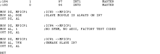
Programming Example #1
Background
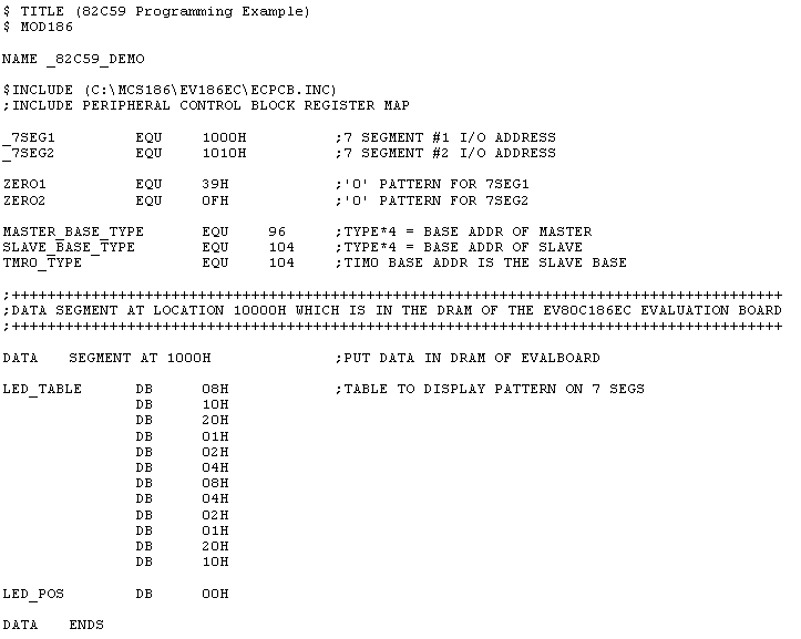
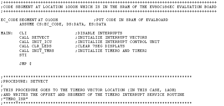
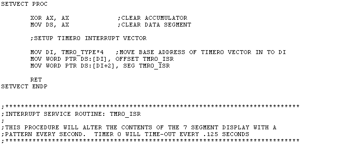
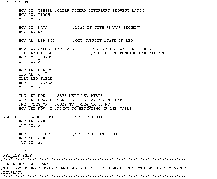
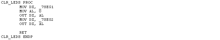
This software example illustrates interrupt vector initialization, basic interrupt controller initialization sequence and a simple interrupt service routine. This software was assembled using Intel ASM86 and was tested using the EV80C186EC Intel evaluation board REV 1.1.

Programming Example #2
Background
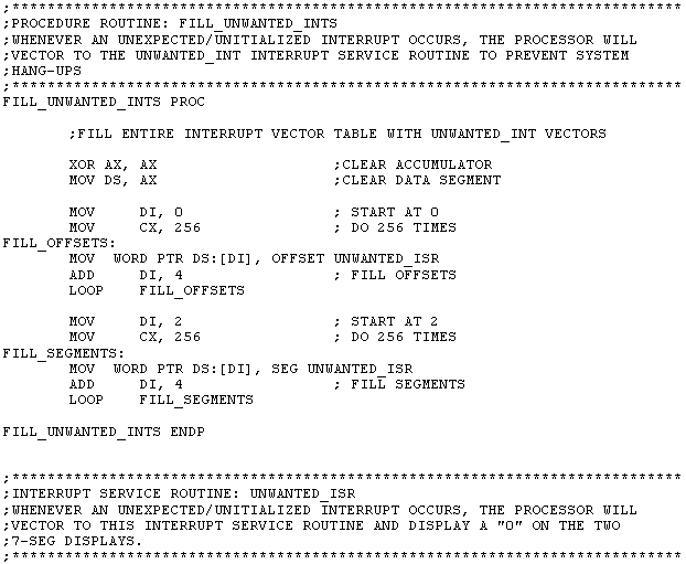
When programming the interrupt control unit, it is important to take unexpected events into consideration. It is possible for an interrupt to occur that was not intentional or unwanted and therefore software should exist to prevent system failure.
The following two subroutines can be used to direct unused interrupts to a common interrupt service routine where they can be handled appropriately to return control back to the main program. These subroutines were not added in Programming Example #1 because the evaluation board firmware already compensates for unwanted interrupts.

Legal Stuff © 1997 Intel Corporation
