The i960 CF processor is code-compatible with all family members, including the entry-level i960®Sx series processors with 16-bit external bus and the mid-range i960®Kx series processors. The i960®CF chip is also socket-compatible with the i960®CA processor, allowing quick design upgrades.
The i960®CF device is targeted for embedded control tasks requiring efficient and fast data movement. Potential applications include internetworking devices, laser printers and high speed I/O control.
i960®CF Processor Features
The i960®CF microprocessor includes the following features:
The i960®CA processor was the first to make use of superscalar design techniques. Simply stated, a superscalar processor makes use of multiple parallel execution units to execute more than one instruction per clock. For example, consider the following sequence of high-level language statements:
a = 2*b + 16*c
d = 4*c + f
A simple scalar processor would execute a sequence of low-level instructions similar to the following:
a = 2*b
temp = 16*c
a = a + temp (# the value for a is solved)
d = 4*e
d = d + f (# the value for d is solved)
If each step took one clock, the entire operation would take five clock cycles. The i960®CF processor, by comparison, would perform the same operation in just two clock cycles. A little background on the internal architecture of the i960®CF processor helps explain the performance improvement.
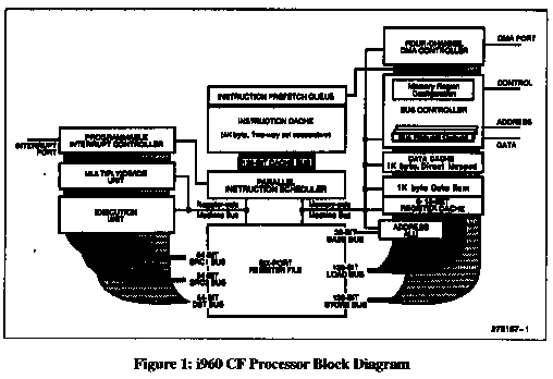
The i960®CF microprocessor has a total of five independent execution units. The Arithmetic Logic Unit (ALU) can perform all of the common arithmetic and logical operations on data stored in the general purpose registers. The Address Generation Unit (AGU) performs the address calculations for LOAD and STORE instructions and can also perform adds and simple multiples on register data. The Bus Controller Unit (BCU) handles all LOAD and STORE instructions. The Multiply/Divide Unit(MDU) accelerates the performance of multiply and divide instructions. Finally, the Instruction Fetch/Decode Unit(IFU) handles program branching instructions.
For the previous example, the i960®CF processor would execute the following code:
a = 2*b, d = 4*e + f
a = a + 16*c
By automatically taking advantage of two of its parallel processing units, the i960®CF processor executes more than one instruction per clock. The instruction "a = 2*b" is issued to the arithmetic logic unit (ALU) while the instruction "d = 4*e + f" is dispatched to the address generation unit, which does double duty as a "mini" ALU. Since the results of the intermediate calculations for "a" and for "d" do not depend on one another, it is possible for the processor to perform the simultaneously.
Had the results of the calculations been dependent on one another, the Instruction Fetch/Decode Unit would have recognized this and prevented parallel execution. The IFU is constantly checking ahead in the instruction stream to determine which instructions can be executed in parallel. Up to three separate instructions may be issued in one clock cycle by the IFU.
Current compiler technology (the Intel iC-960 compiler or Intel's GNU* software tools) makes excellent use of the superscalar capability of the i960®CF device. The compiler is completely aware of the parallel processing units on the microprocessor and takes full advantage when creating its object code.
Advanced Instruction Cache Architecture: When More Isn't Necessarily Better
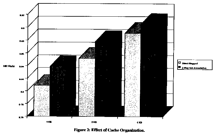
Cache organization refers to the method of assigning locations in main memory to locations in the cache. The instruction caches available on most embedded RISC processors are direct mapped caches. In a direct mapped cache, a specific location in main memory can only be stored in one specific location in the cache. A two-way set associative cache organization allows a specific location in main memory to be stored in one of two locations in the internal cache.
Academic studies have proven that a two-way set associative cache is typically as efficient as a direct mapped cache of twice the size (Computer Architecture A Quantitative Approach, Hennesy & Patterson. 1990). In Figure 2, cache hit rates are plotted for both types of cache organization. Compared, the hit rates of two-way set associative caches and those of a direct mapped cache of twice the size are approximately equal.
Microprocessors with on-chip instruction caches can often have non-deterministic response to real-time events. It is impossible to know if an interrupt procedure will be in the on-chip cache when an interrupt request comes in. The i960®CF processor solves this problem by allowing critical sections of code, such as interrupt handlers, to be permanently locked in the instruction cache. The result: faster and more deterministic interrupt response time.
Data Cache and Data RAM:
Having Your Data Around When You Need It
The i960®CF processor provides a 1 Kbyte direct mapped data cache. The inclusion of a data cache is a significant performance enhancement for applications that keep most of their data in relatively slow DRAM. A data cache also helps bus-intensive multiprocessor applications such as internetworking. While the processor is accessing data in the internal caches, the memory bus is free for use by external agents such as Ethernet and Token Ring controllers.
The on-chip data RAM is a unique feature of the processor. A configurable 1 Kbyte region of zero wait state memory is provided for data variables, local register caching, and interrupt vector storage. The data RAM can be accessed 128 bits (quad word) at a time by the CPU, thus allowing for extremely fast data movement. Unlike a data cache, variables can never be "kicked out" of the data RAM. The iC-960 compiler can take advantage of the on-chip data RAM for critical variable storage, providing high speed and deterministic access to data.
Enhanced Multiply Performance:
More Than Just Fast Calculations
Another i960®CF processor enhancement is the Multiply/Divide Unit (MDU). Where most RISC processors give little or no acceleration to multiply instructions, the i960®CF processor adds an entire functional unit dedicated to performing integer multiply and divide instructions. Multiplication is critical in the following areas:
Choosing which peripherals to integrate is always a difficult task for microprocessor design engineers. Integrate too little and the system hardware design becomes difficult; integrate too much and the end customer cannot differentiate its products. Before deciding upon integration for the i960®CA and i960CF processors, Intel performed an extensive survey of its customer base to determine the most effective integration mix. Two on-chip peripherals were chosen: a four channel DMA controller and an eight-channel expandable interrupt control unit.
The four-channel DMA unit greatly simplifies system design by removing the burden of implementing an off-chip 32-bit DMA controller. DMA is ideal for high-speed I/O peripherals such as networking controllers, video serializers and SCSI ports. The DMA controller supports several modes of operation, including chaining, which is extremely useful for buffer management.
Most real-time systems must deal with multiple interrupt sources. The on-chip interrupt controller allows the direct connection of up to eight interrupt sources. Alternatively, the interrupt controller can accept an 8-bit interrupt vector type, effectively increasing the interrupt handling capability to 256 sources.
Conclusion
The new i960®CF processor represents the continued performance evolution of the i960®architecture. With nearly twice the performance of the i960®CA processor, the i960®CF microprocessor is poised to bring a new level of performance to embedded RISC computing.
*Intel Corporation's GNU960 compiler is based on tools available from the Free Software Foundation.

Legal Stuff © 1997 Intel Corporation