Andrew Swaneck
Flash Product Engineer
Intel Corporation
Vandana Verma
Sr. Technical Marketing Engineer
Intel Corporation
A microprocessor is used in the VAS for acquiring and recording data. The processor's bus interface to Fast Memory is described. Hybrid Flash technology utilizes two different Flash memory components which have high read/write performance. These components are designed into the VAS with scratch pad memory providing a memory solution optimizing speed, cost and density. This optimized memory is called Fast Memory.
Vandana Verma is a Sr. Technical Marketing Engineer at Intel Corporation's Special Markets Division. She is responsible for new Flash product offerings for the Special Environment Marketplace. She has a Master's degree from Arizona State University and started work at Intel as a product engineer. Current responsibilities include writing application notes, white papers; technical documents; training customers on Flash products; developing reference designs, developing software solutions; and helping solve any technical issues that customers may have.
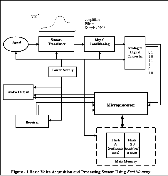
As depicted in Figure-1, signals can be received in multiple file format; either physical voice inputs or direct digital waves. Signal conditioning is performed by amplifiers and filters reducing background noise in the case of direct physical inputs and augmenting faint or distant signals [3]. An A/D converter quantizes the analog signal into meaningful digital components [4]. The microprocessor maintains system control, engaging amplifiers and filters as necessary, as well as providing feature enhancements such as silence compression, gain control, encryption, and message storage [5]. The VAPS main memory consists of both synchronous and asynchronous flash memory components. The two traditional modes of memory storage required by microprocessor based systems are temporary and fixed. Random Access Memory (RAM) is traditionally used for temporary storage, holding data until it is replaced by another microprocessor operation or power is discontinued. Only Memory (ROM) is used for permanent storage . This traditional system RAM and ROM configuration can be replaced with Flash devices. This implementation of Flash for main memory is revolutionary and termed Fast Memory.
More esoteric coding schemes involve vector quantization or the use of memory stored waveform templates to match-up with a set of incoming waveform samples [10].
The flexibility of using a microprocessor in conjunction with flash memory allows a multitude of digitization and coding techniques to be employed. Additionally in-system algorithimic or system coding updates can be performed remotely to the resident Flash memory. Our VAPS can use any processor that has a burst capability or pipeline mode. This capability permits the user to save memory cycles by providing information in parallel on the data bus. This VAPS takes advantage of the burst capability (or pipeline mode ) of processors, providing faster memory accesses. If users would take advantage of this capability, a paradigm shift can be made from needing temporary and fixed memory, namely RAM and ROM, to an exclusive Flash memory system.
The nonvolatile memory technology grew out of the industry's response to the either/or limitations of only RAM and ROM operations. Nonvolatile memory technologies were developed as a result of the industries efforts to improve solid state ROM. Nonvolatile memory is able to retain information after the power is removed from the system and include ROMs, PROMs, EPROMs, EEPROMs and Flash.
ROM is nonvolatile and retains data after the power is removed. Solid state mask ROM devices are fixed memories; each cell in the fixed memory's mask or fuse structure determines it's data content and is unalterable. Traditionally, Erasable Programmable Read Only Memories (EPROMs) handled code and BIOS storage; Electrically Erasable Programmable Read Only Memories (EEPROMs) then replaced anything from Static Random Access Memories (SRAMs) to EPROMs when flexibility and nonvolatility was required at low densities.
The EPROM, although it operates at 5V, requires a powerful electrical pulse for programming, necessitating the use of an additional 12 V power supply. EPROMs can be erased only by using strong ultraviolet (UV) light. Erasure times range from 20 to 50 minutes, depending on the light intensity. The primary benefit of EPROM to the end user is not the rated life cycle but that designs based on these technologies can be changed or updated before a product is released in the market. Although, once released to the marketplace, in system updates are cumbersome, prematurely obsoleting the system due to changing industry standards. EPROM is usually considered a bulk erasable technology because it's complete erasure occurs when it is exposed to UV light. EPROMs are programmed with unique algorithms based on the physical requirements of the manufacturer's process. EPROM is best in applications where data modifications are not required. EEPROM refers to a function or operation, not a single design. Vendors market several different types of EEPROM. EEPROMs are similar to EPROMs requiring strong programming currents but they also incorporate electrical erasure. Erasing before programming each byte, the programming and erase processes occur very fast requiring high internal voltages (e.g. 18V - 30V). The combination of higher voltage with programming and erasing through the same junction contributes to EEPROMs oxide breakdown, poor data retention and reduced cycling capability. EEPROMs technology is designed for selective erasure where each cell can be erased individually. EEPROM is limited in density because of it's selectable byte erasure structure.
Flash memory demonstrates the technical ability to displace each of the existing memories to a varying degree. The name Flash describes the technology's operation because it takes less than five seconds to erase and reprogram and can be done in-socket. Flash technology falls between EPROM and EEPROM in terms of a number of design, operating, and market parameters. With properties that include high speed, nonvolatility and in-system updateability. Flash memory combines the high speed of DRAM, the nonvolatility of hard drives and floppy disk drives, the updateability of RAM or EEPROM, and the high density of ROM. Flash memory has electrical erase capability similar to EEPROM. By using block erasure instead of EEPROMs byte erasure, erase times are relaxed reducing internal voltages. These features for erase and programming provide Flash memory with high reliability and lower failure rates over multiple program / erase cycles. Erase and program verification methods ensure the data integrity of newly altered memory bits.
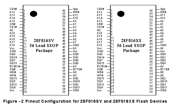
Additionally the address signal A1, controls the selection of odd and even memory banks within the SFI device. The A0 address line is not utilized for either Flash device in word mode. Both the SFI and SV utilize two chip enable control signals (CE0# and CE1#) allowing multiple devices to be connected to the same data bus reducing the amount of control circuitry used for decoding chip selections. Other control signals consist of OE# (Output enable - data reads),and WE# (Write Enable - data writes). The SFI and SV have flexibility in the choice of power supply configurations. These devices exhibit good read performance with either a 3.3V or a 5.0V supply voltage and program / erase compatibility with either a 5.0V or a 12.0V programming voltage. The flexibility to use lower voltages in designs eliminates the need for external voltage converters and regulators and enhances compatibility with hand held battery applications. These devices also incorporate low power modes, further reducing power consumption. For instance, in the SV, these modes are standby, deep powerdown, and sleep [12]. Standby and deep powerdown modes are controlled by device pins CE0# / CE1# and RP# respectively; sleep mode, similar to deep powerdown, is software controlled by writing either command codes F0H or 80H to the device. Table-1 shows a comparison of device power consumption across variations in supply voltage and device configurations.
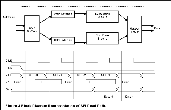
The main difference in features between the SFI and SV Flash devices is the design of the read path. The SV is an asynchronous main memory device in which device data becomes valid sometime after a corresponding address transition. In the case of the SV device access times are 65-70nsec [13]. The SFI, on the other hand, utilizes a synchronous pipeline architecture containing two additional control signals CLK (Clock) and ADV# (Address Valid). These two signals are used in conjunction with address memory when reads are initiated. Figure-3 shows a block diagram representation of the SFI read path and corresponding device timing waveforms [13]. As shown in Figure 3, valid addresses are
Table-1 Power Consumption versus Supply Voltage and Device Operating Modes [13]:
| Operating Mode | Vcc = 3.3V Vpp = 5.0V |
Vcc = 5.0V Vpp = 5.0V |
Vcc = 3.3V Vpp = 12.0V |
Vcc = 5.0V Vpp = 12.0V |
|---|---|---|---|---|
| Powerdown | 7.6uW | 11uW | 9uW | 12.4uW |
| Standby | 380uW | 500uW | 590uW | 700uW |
| Read Mode | 130mW | 375mW | 130mW | 375mW |
latched into the device on the rising edge of the clock signal with the address valid (ADV#) control signal low. Subsequent clock cycles continue to latch new memory address locations. By alternating even and odd address banks using the A1 bank select address signal, data is pipelined through the device. Effectively after 3-clock cycles, valid data based upon the first clocks memory address location becomes valid on the data bus. This configuration has the unique advantage of coordinating data accesses and reducing the overall access time. Equivalent access times of up to 30 nsec an be achieved using this configuration [13]. The addition of the ADV# control signal allows the SFI device to run at higher clock speeds. When the address valid control signal is toggled high, data reads are prohibited. This allows the user to insert delays or "wait states". Clock frequencies of up to 66 Mhz can be used with the SFI device, by controlling address accesses using the ADV# control signal.
Another difference between the SFI and the SV flash devices is the incorporation of SRAM-like memory internal to the SV. on board memory consists of two 256 byte "page buffers", providing on-chip virtual memory storage for data writes to the flash memory array [14]. 512 bytes of data can effectively be queued into the page buffers before a flash write command needs to be issued. This improves device programming and data storage efficiency by a factor of 5X over directly programming the flash array [14]. Both the SFI and SV Flash devices contain a Write State Machine (WSM) which utilizes a command user interface (CUI) controlling Flash device operations. These commands initiate internal program and erase algorithms, internally controlling the write and erase functions of the device. Tables 2 and 3 show a list of the user commands available and their functions [14].
Table 2. SFI / SV Command Codes [14]
| Command | Oper | Addr | Data | Oper | Addr | Data | Oper | Addr | Data |
|---|---|---|---|---|---|---|---|---|---|
| Read Array | Write | X | FFH | Read | AA | AD | |||
| Intelligent Identifier | Write | X | 90H | Read | IA | ID | |||
| Read CSR | Write | X | 70H | Read | X | CSR | |||
| Clear Status Register | Write | X | 50H | ||||||
| Word / Byte Write | Write | X | 40H | Write | WA | WD | |||
| Alternate Word Byte Write | Write | X | 10H | Write | WA | WD | |||
| Block Erase / Confirm | Write | X | 20H | Write | BA | D0H | |||
| Erase Suspend / Resume | Write | X | B0H | Write | X | D0H | |||
| Read Ext. Status Register | Write | X | 71H | Read | RA | GSR/BSR | |||
| Lock Block / Confirm | Write | X | 77H | Write | BA | D0H | |||
| Upload Status Bits / Confirm | Write | X | 97H | Write | X | D0H |
Table 3. SV Specific Command Codes
| Command | Oper | Addr | Data | Oper | Addr | Data | Oper | Addr | Data |
|---|---|---|---|---|---|---|---|---|---|
| Read Page Buffer | Write | X | 75H | Read | PA | PD | |||
| Single Load to Page Buffer | Write | X | 74H | Write | PA | PD | |||
| Seq. Load Page Buffer | Write | X | E0H | Write | X | BCL WCL | Write | X | BCH WCH |
| Page Buffer Swap | Write | X | 72H | ||||||
| Page Buffer Write to Flash | Write | X | 0CH | Write | A0 / X | BC(L,H) WCL | Write | WA | BC(H,L) WCH |
| Two-Byte Write | Write | X | FBH | Write | A0 | WD(L,H) | Write | WA | WD(H,L) |
| Upload Device Information | Write | X | 99H | Write | X | D0H | |||
| Erase all Unlocked Blocks | Write | X | A7H | Write | X | D0H | |||
| RY/BY# Enable to Level | Write | X | 96H | Write | X | 01H | |||
| RY/BY# Pulse-on-Write | Write | X | 96H | Write | X | 02H | |||
| RY/BY# Pulse-on-Erase | Write | X | 96H | Write | X | 03H | |||
| RY/BY# Disable | Write | X | 96H | Write | X | 04H | |||
| RY/BY# Pulse Write/Erase | Write | X | 96H | Write | X | 05H | |||
| Sleep | Write | X | F0H | ||||||
| Abort | Write | X | 80H |
| ADDRESS: | DATA: | |
| AA = Array Address | AD = Array Data | WC (L,H) = Word Count ( Low / High) |
| PA = Page Buffer Address | PD = Page Buffer Data | BC (L,H) = Byte Count ( Low / High) |
| RA = Ext. Register Address | BSRD = BSR Data | WD (L,H) = Write Data ( Low / High) |
| WA = Write Address | GSRD = GSR Data | |
| X = Don't Care | DCCD = Configuration Code Data | |
| BA = Block Address | WD = Word Data | |
Device status is provided by three status registers namely Block Status Register (BSR), Global Status Register (GSR), and Compatible Status Register (CSR).
Legal Stuff © 1997 Intel Corporation
