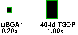
This paper discusses Intel's next-generation CSP package, the µBGA* package. This package clearly enables Intel to respond to customer needs for smaller and thinner flash memory components. For example, the diagram above illustrates the board space comparison between a 0.4µ technology 8-Mbit Intel Flash memory in a 40-bump (5x8 matrix) µBGA package and the same device in 40-lead TSOP. Reducing the size of the package to address our customers' requirements was a key factor in Intel's decision to pursue a CSP. However, that was only part of the decision process; other key factors were also considered prior to Intel choosing the µBGA package over other CSP alternatives.
Additional Factors Considered
In making the decision to develop and deploy the µBGA package for flash memory, some additional areas considered include the following.
1) The package chosen had to match (or ideally exceed) both our customers' quality and reliability expectations and the excellent quality and reliability levels associated with our existing smallest package option, TSOP.
2) The package should leverage the current investment that our customers have made in both PCB technology and board assembly equipment. In addition the potential of it being an industry-wide solution should be considered.
3) The package deployment schedule had to meet or exceed our customers' timeframe expectations for this type of solution.
4) The cost of assembling the package in the future was considered, so as to meet our customers' cost expectations. This includes the ability to cost reduce and be competitive, if not superior, to other solutions.
5) As an additional factor in total cost, the cost of deploying the package in Intel's assembly and test facilities was considered.
Intel's internal analysis, as well as that of customers and vendor partners, confirms that the µBGA package meets or exceeds all expectations in each of these focus areas; a true win-win for Intel, its customers and their end users! The following sections will cover each focus topic in more detail.
Smallest Package Size
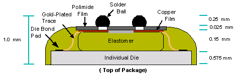
The µBGA package is a true die-sized package. In addition, the matrix of solder balls for mounting the component to the PCB allows for routing to occur
underneath the package using standard PCB trace/space design rules. Thus, the total footprint for the package on the board is as small or smaller than any other
CSP. In addition, this routing technique will quite often result in a smaller footprint than a die solution. By choosing the µBGA package over other CSPs, customers
will have the smallest-possible footprint available.
High-Quality And High-Reliability For Portable Environments
A key factor considered by Intel when contemplating bringing a new package to production is its quality and reliability potential. A major area of focus is the solder
joint reliability of the package/board system. The µBGA package's compliant elastomer relieves the stress caused by any CTE (thermal coefficient of expansion)
mismatch between the silicon die and the PCB, ensuring reliable long-term solder joint integrity. This is very important when one considers that the focus
applications for this package include portable communications and computing systems. By their very nature, these systems will be operated in a variety of
environments and with less-than-optimal end user handling characteristics. Intel believes that the µBGA package design offers the best solder joint performance of
the available CSP choices for flash memory. In addition, the µBGA package design will not require the additional complexity and cost of doing underfill, required for
some CSP alternatives.
One other factor considered regarding quality was the customers' PCB assembly failure rate expectations. BGA-type packages intrinsically have self-aligning qualities during soldering, which equate to lower assembly defects. BGA packages are also leadless, again simplifying handling requirements and optimizing yield.
Leverages Existing SMT Technology
The analysis and feedback we received from customers and vendors alike indicates that given the µBGA package's pitch and ball count/matrix dimension
characteristics, they will be able to cost-effectively implement the package using existing single-layer PCB design technology. They also believe that the µBGA
package will integrate into their presently installed surface mount assembly capability with little or no incremental learning curve, process changes or equipment
investments. Pick-and-place equipment and the present IR reflow profiles for TSOP are also projected to work for the µBGA package with minimal adjustments.
Industry-Standard Solution
Intel also considered the ability of others to adopt the package, specifically the potential that the package would become a broadbase industry standard. With the
µBGA package being a compelling third-party offering, it was felt that others would have easier access to the core package technology. In fact, the 0.75 mm pitch
µBGA package specification that Intel will use for flash memory has been registered for publication at JEDEC (MO-195); an important industry statement. Intel and
others are also currently pursuing approval at other industry standards bodies.
Timely Solution For Customer's System Schedules
Intel's decision to go with the µBGA package was heavily influenced by the resultant ability for Intel to deliver a solution that met our customers' required sampling
and production schedules. Our customers wanted a robust solution for their designs beginning in 1997. The µBGA package is predicted to provide a
state-of-the-art solution for flash memory packaging in that timeframe. Intel's Flash Memory Component Division has an excellent track record of deploying
compelling solutions and driving continuous cost improvements for those solutions. For example, Intel was the leader in introducing TSOP for flash memory six
years ago. Today, Intel is also the volume leader and quality leader for flash memory in TSOP.
Best-Of-Class Assembly Cost Solution
In addition to the time-to-market factors involved in introducing a package, Intel also strongly considered the cost reduction potential of the package technology in
the future. Intel believes that the potential to cost-reduce the assembly process of the µBGA package will quickly make it as cost-effective as the TSOP solution is
today.
Cost-Effective Test Process Implementation
Intel also considered our ability to provide quality testing to a device in the µBGA package and the cost of implementing it into our existing test process. In both
cases, Intel believes that the µBGA package is a solid choice. Intel will be able to test the µBGA-packaged product to the same test flow we currently use for our
TSOP offerings. Intel will also be able to leverage the current equipment base we have as well as the experience we have with that equipment.
Conclusion
Intel considered a number of factors before deciding to deploy the µBGA package. Intel believes it has chosen a superior package from a size, quality/reliability,
implementation and time-to-market standpoint. In addition, the µBGA package has already received JEDEC registration approval and work is underway to extend
this to other standards bodies. Finally, Intel also believes it has made the best choice when considering cost of component assembly and taking into account our
customer's ease-of-use expectations.
* All other company, brand and product names are trademarks or registered trademarks of their respective companies.
Legal Stuff © 1997 Intel Corporation
